Semiconductor memory device and driving method thereof

a memory device and semiconductor technology, applied in the direction of information storage, static storage, digital storage, etc., can solve the problems of power consumption, power consumption, and skew between the external clock signal and the internal clock signal, so as to minimize the power consumption of the semiconductor memory device and increase the power consumption

Active Publication Date: 2010-11-04
SK HYNIX INC
View PDF5 Cites 8 Cited by
  • Summary
  • Abstract
  • Description
  • Claims
  • Application Information

AI Technical Summary

Benefits of technology

[0018]An embodiment of the present invention is directed to providing a semiconductor memory device which can limit counting operation during a write operation interval of a semiconductor memory device.
[0021]In accordance with another aspect of the present invention, there is provided a method for driving a semiconductor memory device, which includes: counting a DLL clock signal and an external clock signal by being reset in response to an output enable reset signal; latching a value obtained by counting the external clock signal, in response to a read command that is activated in read operation; comparing the value latched in latching and a value obtained by counting the DLL clock signal, and generating an output enable signal corresponding to an operating frequency; and performing write operation while preventing counting of the DLL clock signal and the external clock signal in response to a write command.
[0022]A conventional output enable signal generation circuit performs counting operation in read and write operation of a semiconductor memory device, and due to this fact, power consumption increases. However, since an output enable signal is used only in the read operation of the semiconductor memory device, it is not needed during a write operation interval. That is to say, the output enable signal generation circuit can be inactivated during the write operation interval. In the present invention, an output enable signal generation circuit which is inactivated during a write operation interval is provided, whereby it is possible to minimize power consumption of a semiconductor memory device.

Problems solved by technology

Meanwhile, a skew may occur between the external clock signal and the internal clock signal due to delay factors in the semiconductor memory device.
The counting operation consumes power.
Namely, the semiconductor memory device performs counting operation in read and write operation, whereby power consumption occurs.

Method used


Image

  • Semiconductor memory device and driving method thereof
  • Semiconductor memory device and driving method thereof
  • Semiconductor memory device and driving method thereof

Examples


Embodiment Construction

[0028]Other objects and advantages of the present invention can be understood by the following description, and become apparent with reference to the embodiment of the present invention.

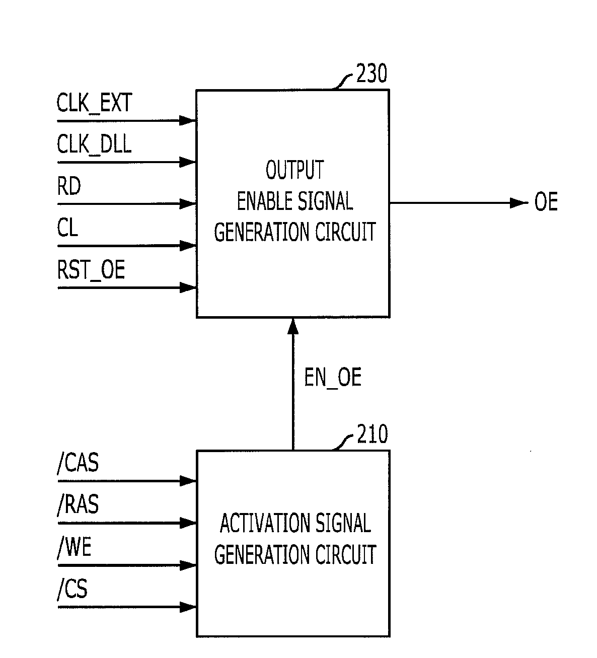
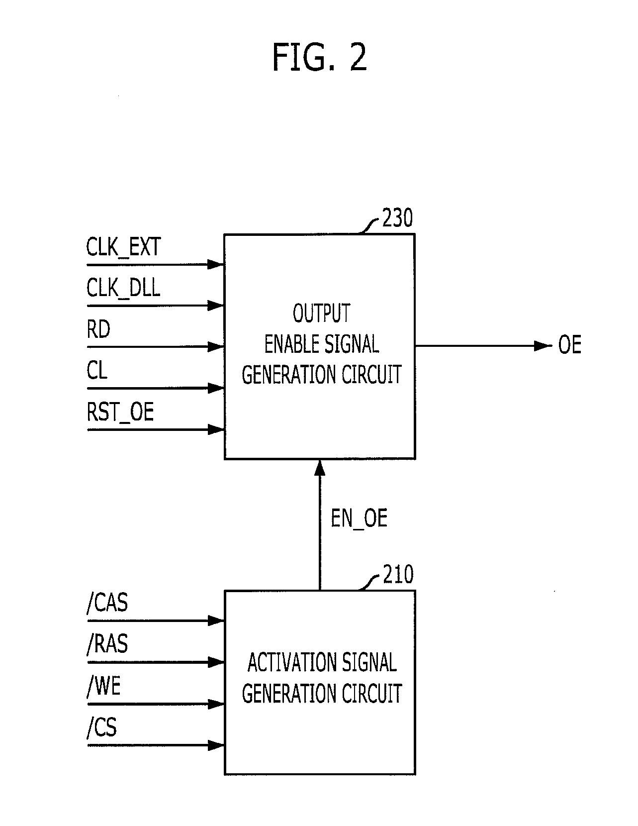
[0029]FIG. 2 is a block diagram illustrating a partial configuration of a semiconductor memory device in accordance with an embodiment of the present invention.

[0030]Referring to FIG. 2, a semiconductor memory device includes an activation signal generation circuit 210 and an output enable signal generation circuit 230.

[0031]The activation signal generation circuit 210 generates an activation signal EN_OE for inactivating the output enable signal generation circuit 230 during a write operation. The activation signal generation circuit 210 generates the activation signal EN_OE in response to a column address strobe signal ( / CAS), a row address strobe signal ( / RAS), a chip select signal ( / CS) and a write enable signal ( / WE). The column address strobe signal ( / CAS), the row address strobe signal ( / RAS),...


PUM


Abstract

A semiconductor memory device includes output enable signal generation means configured to be reset in response to an output enable reset signal, count a DLL clock signal and an external clock signal, and generate an output enable signal in correspondence to a read command and an operating frequency; and activation signal generation means configured to generate an activation signal for inactivating the output enable signal generation means during a write operation interval.

Description

CROSS-REFERENCE TO RELATED APPLICATIONS[0001]The present application claims priority of Korean Patent Application No. 10-2009-0038528, filed on Apr. 30, 2009, the disclosure of which is incorporated herein by reference in its entirety.BACKGROUND OF THE INVENTION[0002]The present invention relates to a semiconductor design technique, and more particularly, to a semiconductor memory device which generates an output enable signal and performs data input and output operation using the output enable signal.[0003]In general, a semiconductor memory device such as a double data rate synchronous DRAM (DDR SDRAM) is inputted with a read command synchronized with an external clock signal and outputs data synchronized with an internal clock signal during read operation. That is to say, not the external clock signal but the internal clock signal is used to output data in the semiconductor memory device. Due to this fact, in the read operation, the read command synchronized with the external cloc...

Claims


Application Information

Patent Timeline
Patent Type & Authority Applications(United States)
IPC IPC(8): G11C7/22
CPCG11C7/1051G11C7/222G11C7/22G11C7/1066G11C7/1078G11C7/20G11C11/4072G11C11/4076G11C11/4093G11C11/4096
Inventor NOH, YOUNG-KYU
Owner SK HYNIX INC
Why Eureka
Try Eureka