Solid-state imaging apparatus, driving method of the solid-state imaging apparatus, and electronic equipment

a technology of solid-state imaging and driving method, which is applied in the direction of television system scanning details, radioation control devices, television systems, etc., can solve the problems of degrading resolution and long sideways images, and achieve the reduction of horizontal signal number, frame rate, and angle of view reduction

Active Publication Date: 2010-11-11
SONY CORP
View PDF5 Cites 47 Cited by
  • Summary
  • Abstract
  • Description
  • Claims
  • Application Information

AI Technical Summary

Benefits of technology

[0010]In recent years, the request for high-speed image pickup is more and more increased. In the column AD conversion type CMOS image sensor, the number of vertical readout lines (number of rows / number of lines) is reduced to meet the request. As a method of reducing the number of vertical readout lines, there is a method of interlaced scanning such as, for example, vertical thinning-out readout in which a pixel row is skipped at a constant row period, or vertical segmentation in which signals of pixels in a specific area in the vertical direction are read out. However, there arises a problem that when the number of readout lines is reduced by the thinning-out readout, the resolution is degraded, and when the number of vertical readout lines is reduced by the interlaced scanning, a pickup image becomes long sideways by reduction in angle of view.
[0011]It is therefore desirable to provide a solid-state imaging apparatus in which degradation of resolution at the time of vertical thinning-out readout can be reduced, and it is possible to prevent a pickup image from becoming long sideways by suppressing the reduction in angle of view when pixel rows are interlace-scanned, a driving method of the solid-state imaging apparatus and an electronic equipment.
[0013]The row scanning section simultaneously outputs the drive signals of the pixels to the plural pixel rows in the different pixel columns through the plural systematic pixel drive lines, so that plural pixel rows in the different pixel columns can be simultaneously scanned. By this, with respect to the plural pixel rows, signals are read out from a part of the pixels, not all the pixels of one pixel row. In other words, when attention is paid to one pixel row, signals of a part of pixels are thinned out at the time of signal readout. By this horizontal thinning-out readout, the number of signals in the horizontal direction can be reduced. Thus, as compared with a case where the horizontal thinning-out readout is not performed, the frame rate can be increased, and when pixel rows are interlace-scanned, the reduction in angle of view can be suppressed.
[0015]The row scanning section simultaneously output the drive signals of the pixels to the plural pixel rows, so that the signals of the pixels are read out to the plural systematic signal lines from the plural pixel rows. At this time, when one of the plural systematic signal lines is selected for each pixel column, with respect to the plural pixel rows, signals are read out from a part of pixels, not all the pixels of one pixel row. In other words, when attention is paid to one pixel row, signals of a part of pixels are thinned out at the time of signal readout. By this horizontal thinning-out readout, the number of signals in the horizontal direction can be reduced. Thus, as compared with the case where the horizontal thinning-out readout is not performed, the frame rate can be increased, and when pixel rows are interlace-scanned, the reduction in angle of view can be suppressed.
[0016]According to the embodiments of the present invention, when the pixel rows are interlace-scanned, the horizontal thinning-out readout is performed, so that the reduction in angle of view can be suppressed, and therefore, it is possible to prevent the pickup image from becoming long sideways.

Problems solved by technology

However, there arises a problem that when the number of readout lines is reduced by the thinning-out readout, the resolution is degraded, and when the number of vertical readout lines is reduced by the interlaced scanning, a pickup image becomes long sideways by reduction in angle of view.

Method used


Image

  • Solid-state imaging apparatus, driving method of the solid-state imaging apparatus, and electronic equipment
  • Solid-state imaging apparatus, driving method of the solid-state imaging apparatus, and electronic equipment
  • Solid-state imaging apparatus, driving method of the solid-state imaging apparatus, and electronic equipment

Examples


first embodiment

2. First Embodiment

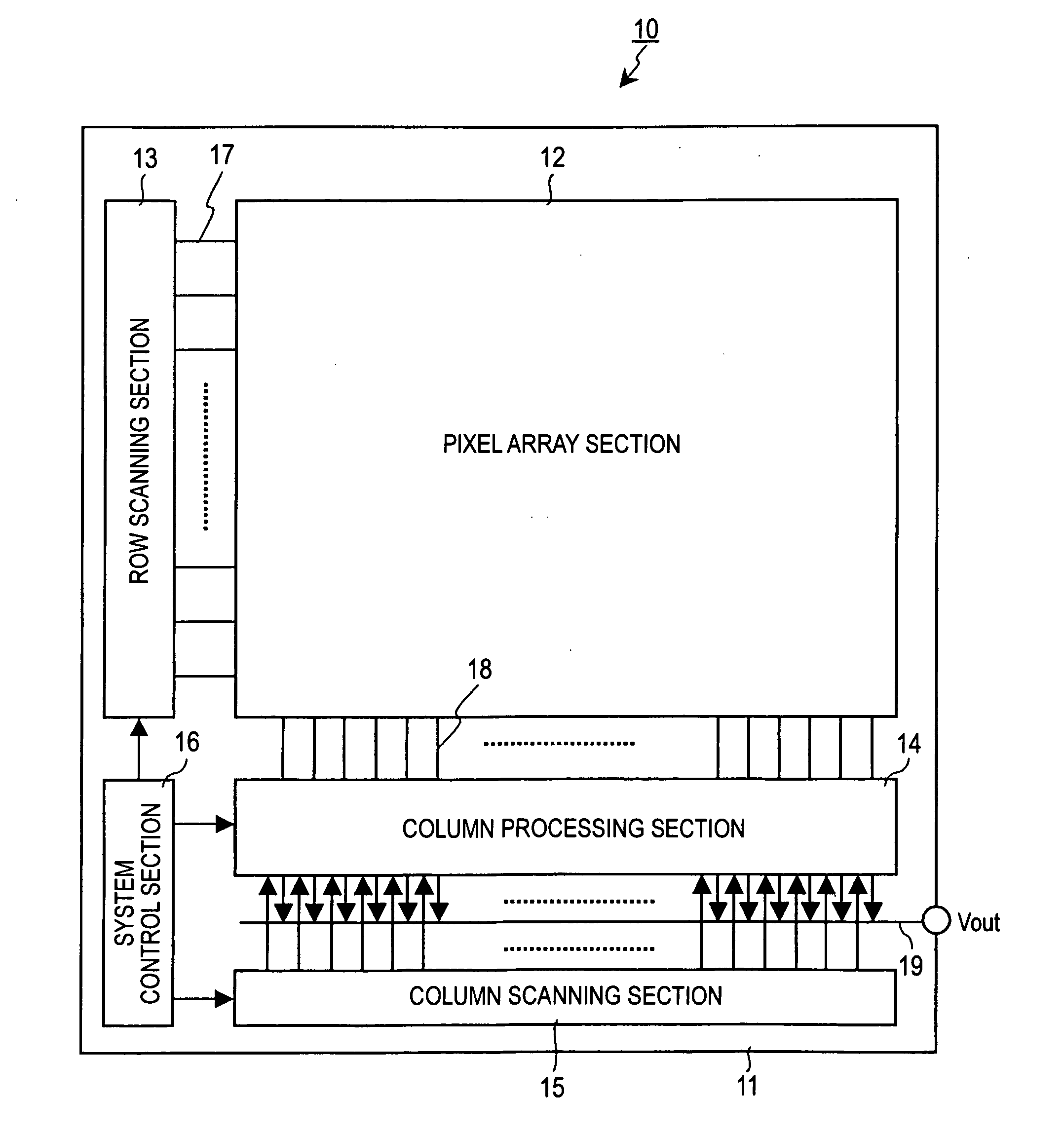
[0063]FIG. 3 is a system structural view showing the outline of a system structure of a CMOS image sensor 10A of a first embodiment of the invention. In the drawing, the same portion as that of FIG. 1 is denoted by the same reference numeral.

[0064]The CMOS image sensor 10A of this embodiment is constructed such that plural, for example, two systematic pixel drive lines 17 are arranged for each pixel row. Unit pixels 20 are connected to the two systematic pixel drive lines 17A and 17B in units of two adjacent columns. Specifically, the connection relation is such that from the left in the drawing, the respective pixels 20 of the first pixel column and the second pixel column are connected to the pixel drive line 17A, the respective pixels 20 of the third pixel column and the fourth pixel column are connected to the pixel drive line 17B, the respective pixels 20 of the fifth pixel column and the sixth pixel column are connected to the pixel drive line 17A, and so on...

second embodiment

3. Second Embodiment

[0104]FIG. 10 is a system structural view showing the outline of a system structure of a CMOS image sensor 10B of a second embodiment. In the drawing, the same portion as that of FIG. 3 is denoted by the same reference numeral.

[0105]The CMOS image sensor 10B of this embodiment has a structure in which plural, for example, two systematic (two lines) vertical signal lines 18 are arranged for each pixel column. Unit pixels 20 are alternately connected to the two systematic vertical signal lines 18A and 18B for the respective pixel rows. Specifically, the connection relation is such that each of the pixels 20 of the first pixel row from above in the drawing is connected to the vertical signal line 18A, and each of the pixels 20 of the second pixel row is connected to the vertical signal line 18B, each of the pixels 20 of the third pixel row is connected to the vertical signal line 18A, and so on.

[0106]One systematic pixel drive line 17 is arranged for each pixel row....

third embodiment

4. Third Embodiment

[0135]FIG. 13 is a system structural view showing the outline of a system structure of a CMOS image sensor 10C of a third embodiment. In the drawing, the same portion as that of FIG. 10 is denoted by the same reference numeral.

[0136]In the CMOS image sensor 10B of the second embodiment, for example, the two systematic vertical signal lines 18A and 18B are arranged for each pixel column. Then, the vertical signal lines 18A and 18B are alternately selected in units of two adjacent columns by the selection switch 143, and the signals are read out simultaneously from the pixels 20 of two pixel rows for different pixel columns, so that the horizontal thinning-out readout is performed while the vertical thinning-out readout is performed.

[0137]The CMOS image sensor 10C of this embodiment is the same as the CMOS image sensor 10B of the second embodiment in that plural, for example, two systematic vertical signal lines 18A 18B are provided for each pixel column, and signal...


PUM


Abstract

A solid-state imaging apparatus includes: a pixel array section in which pixels including photoelectric conversion elements are two-dimensionally arranged in a matrix form, and a plurality of systematic pixel drive lines to transmit drive signals to read out signals from the pixels are arranged for each pixel row; and a row scanning section to simultaneously output the drive signals through the plurality of systematic pixel drive lines to a plurality of pixel rows for different pixel columns.

Description

BACKGROUND OF THE INVENTION[0001]1. Field of the Invention[0002]The present invention relates to a solid-state imaging apparatus, a driving method of the solid-state imaging apparatus and an electronic equipment.[0003]2. Description of the Related Art[0004]An imaging apparatus, such as a digital still camera, to convert light into an electric signal and to output an image signal includes a solid-state imaging apparatus as an image capture section (photoelectric conversion section). In the field of the solid-state imaging apparatus, in recent years, as the number of pixels is increased and a frame rate is raised, a technology of realizing high-speed reading and a technology of realizing low power consumption become essential technologies.[0005]As a type of solid-state imaging apparatus, there is a CMOS (including a MOS) image sensor (hereinafter referred to as “CMOS image sensor”) taking advantage of a feature that it can be manufactured by the same process as a CMOS integrated circu...

Claims


Application Information

Patent Timeline
Patent Type & Authority Applications(United States)
IPC IPC(8): H04N5/335H01L27/146H04N5/341H04N5/369H04N5/374H04N5/378
CPCH01L27/14621H01L27/14627H01L27/14636H01L27/14643H04N5/3456H01L27/1464H04N5/3742H04N5/37455H04N9/045H04N5/378H04N5/3458H01L27/14647H04N25/445H04N25/767H04N25/772H04N25/70H04N25/447H04N25/134H04N25/75
Inventor ARAKI, YUICHIROKIKUCHI, MASARU
Owner SONY CORP
Why Eureka
Try Eureka