Computing systems and methods for managing flash memory device

a memory device and computing system technology, applied in computing, memory adressing/allocation/relocation, instruments, etc., can solve the problems of reducing reading speed and requiring a lot of time for rase operations

Inactive Publication Date: 2010-11-11
INTEL CORP
View PDF3 Cites 247 Cited by
  • Summary
  • Abstract
  • Description
  • Claims
  • Application Information

AI Technical Summary

Problems solved by technology

Thus, an erase operation typically requires much more time than a write and a read operation.
However, in the read operation, a process of visiting (i.e. reading or traversing) the data in a reverse order from the end of the log block is required to retrieve the latest data, which seriously degrades the reading speed due to a huge amount of unnecessary read operation during the reversely visiting.

Method used


Image

  • Computing systems and methods for managing flash memory device
  • Computing systems and methods for managing flash memory device
  • Computing systems and methods for managing flash memory device

Examples


Embodiment Construction

[0027]The following description is of the best-contemplated mode of carrying out the invention. This description is made for the purpose of illustrating the general principles of the invention and should not be taken in a limiting sense. The scope of the invention is best determined by reference to the appended claims.

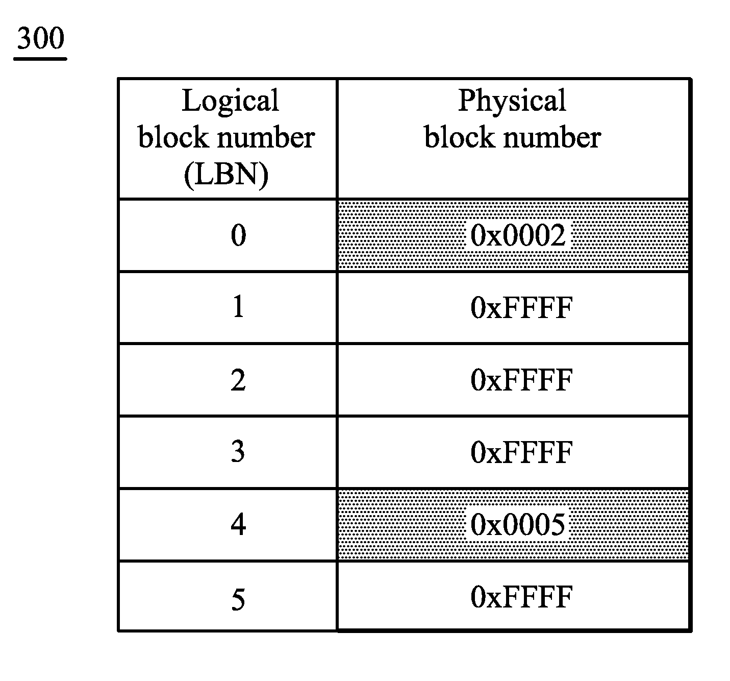
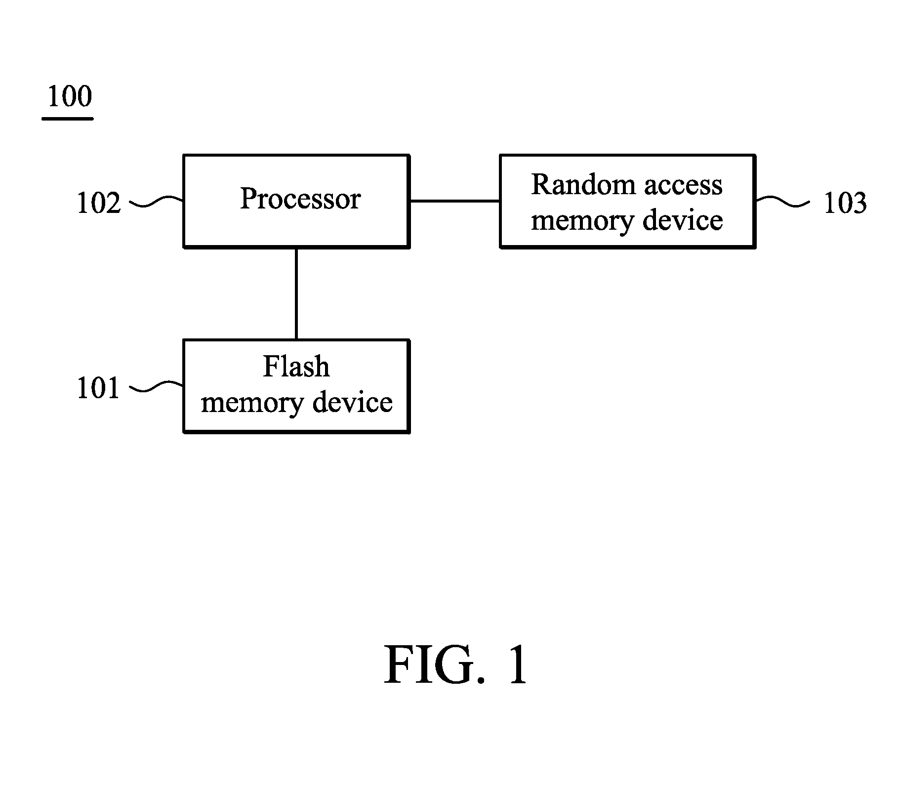
[0028]FIG. 1 shows a computing system 100 according to an embodiment of the invention. The computing system 100 comprises a flash memory device 101, a processor 102 and a random access memory device 103. The processor 102 manages the flash memory device 101 according to the received commands by executing program codes. According to an embodiment of the invention, the flash memory device 101 may be a memory device having the property that in the access operation, size of a minimum erasable memory unit should be larger than size of a minimum writable memory unit. As an example, a NAND flash or a NOR flash. The flash memory device 101 may comprise at least one mapping blo...


PUM


Abstract

A computing system is provided. A flash memory device includes at least one mapping block, at least one modification block and at least one cache block. A processor is configured to perform: receiving a write command with a write logical address and predetermined data, loading content of a cache page from the cache block corresponding to the modification block according to the write logical address to a random access memory device in response to that a page of the mapping block corresponding to the write logical address has been used, the processor, reading orderly the content of the cache page stored in the random access memory device to obtain location information of an empty page of the modification block, and writing the predetermined data to the empty page according to the location information. Each cache page includes data fields to store location information corresponding to the data has been written in the pages of the modification block in order.

Description

CROSS REFERENCE TO RELATED APPLICATIONS[0001]This Application claims priority of Taiwan Patent Application No. 98114956 and China Patent Application No. 200910136521.9, both filed on the same date, May 6, 2009, the entirety of which is incorporated by reference herein.BACKGROUND OF THE INVENTION[0002]1. Field of the Invention[0003]The invention relates to a method for managing a memory device, and more particularly to a method for optimizing read and write operations of a flash memory device.[0004]2. Description of the Related Art[0005]A flash memory or EEPROM (Electrically Erasable Programmable Read Only Memory) is a special type of nonvolatile memory capable of electrically erasing and programming data. In this context, these two terms, flash memory and EEPROM, are usually equivalent and interchangeable. Flash memory based storage devices have low power consumption and small size as compared to magnetic disc memory based devices. Thus, they are often used as storage devices for mo...

Claims


Application Information

Patent Timeline
Patent Type & Authority Applications(United States)
IPC IPC(8): G06F12/00G06F12/10G06F12/08
CPCG06F12/0246G06F2212/7203G06F2212/7202
Inventor LI, RONGWANG, HUAQIAOJIN, YUEFENG
Owner INTEL CORP
Why Eureka
Try Eureka