Electron injection-controlled microcavity plasma device and arrays

Active Publication Date: 2010-11-18
THE BOARD OF TRUSTEES OF THE UNIV OF ILLINOIS
View PDF16 Cites 25 Cited by
  • Summary
  • Abstract
  • Description
  • Claims
  • Application Information

AI Technical Summary

Benefits of technology

[0007]An embodiment of the invention is a microcavity plasma device that can be controlled by a low voltage electron emitter. The microcavity plasma device includes driving electrodes disposed proximate to a microcavity and arranged to contribute to generation of plasma in the microcavity upon application of a driving voltage. An electron emitter is arranged to emit electrons into the microcavity upon application of a control voltage. The electron emitter is an electron source having an insulator layer

Problems solved by technology

Plasma display panel technology, on the other hand, requires a partial vacuum in the display which requires accordingly sturdy packaging to protect the panels.
Switching high voltages directly requires relatively expensive driving electronics.
The circuitry for switching the high voltages represents a significant cost in the manufacturing of existing plasma televisions, for example.
The need for high speed and high

Method used


Image

  • Electron injection-controlled microcavity plasma device and arrays
  • Electron injection-controlled microcavity plasma device and arrays
  • Electron injection-controlled microcavity plasma device and arrays

Examples


Embodiment Construction

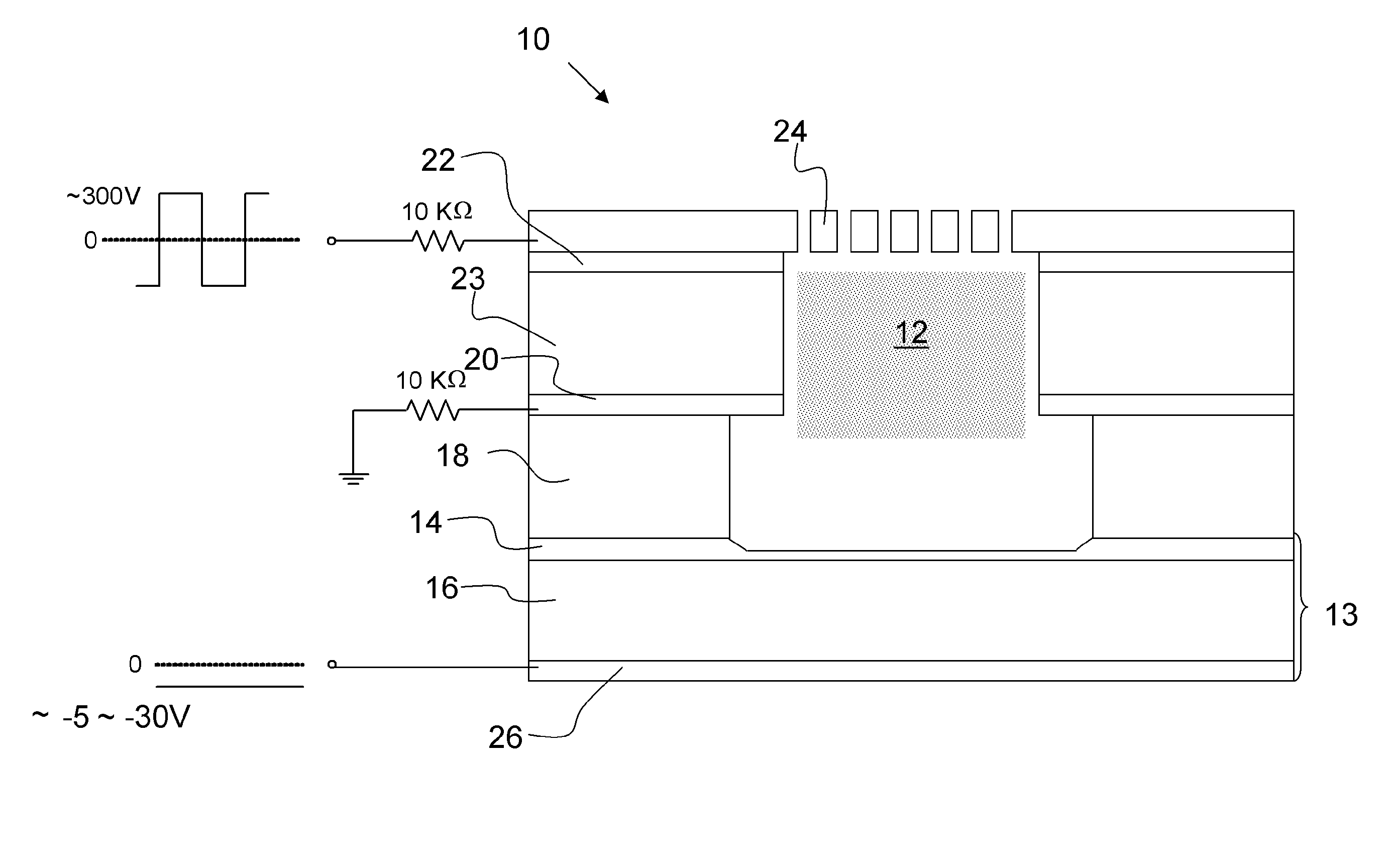
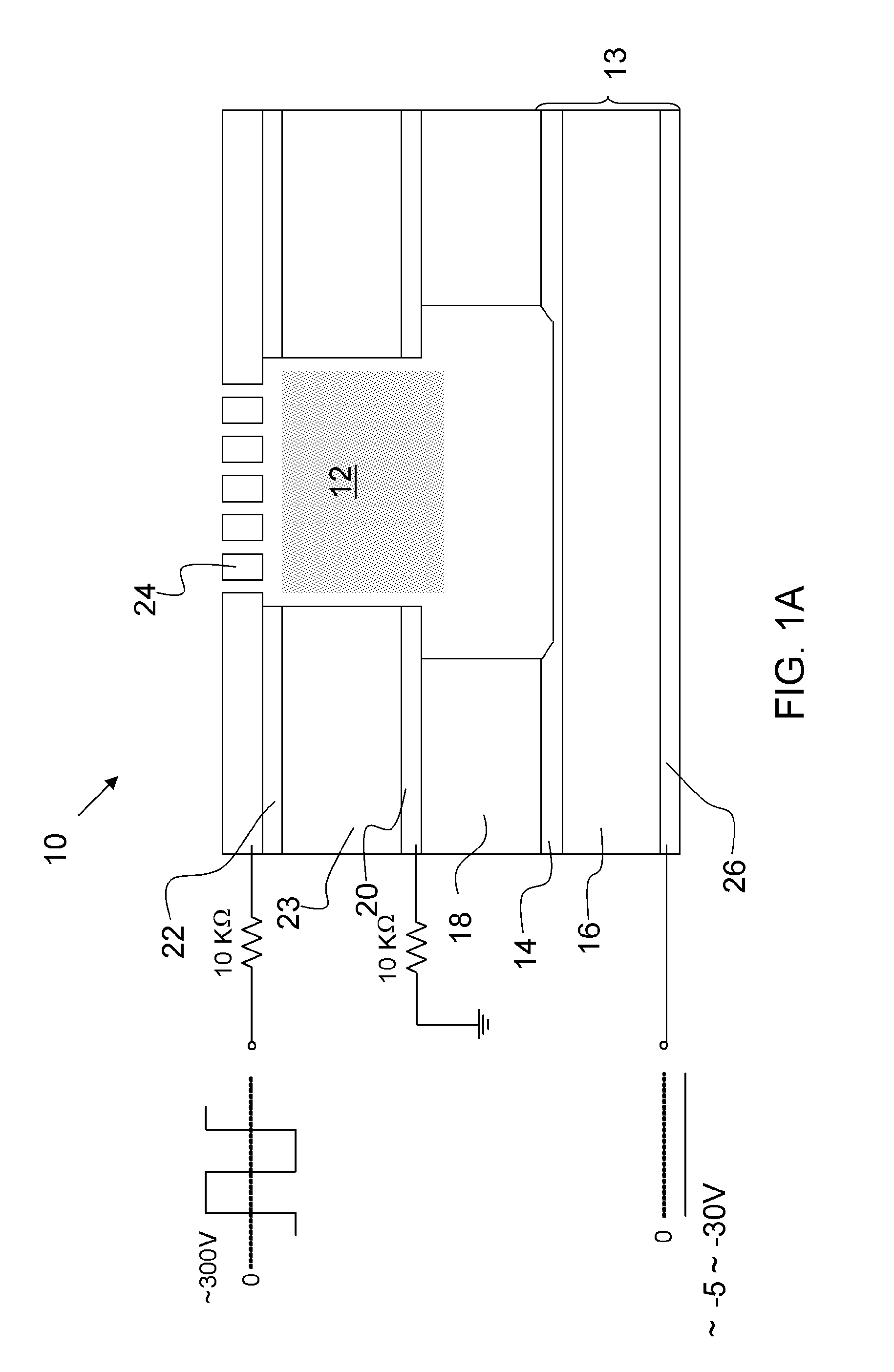
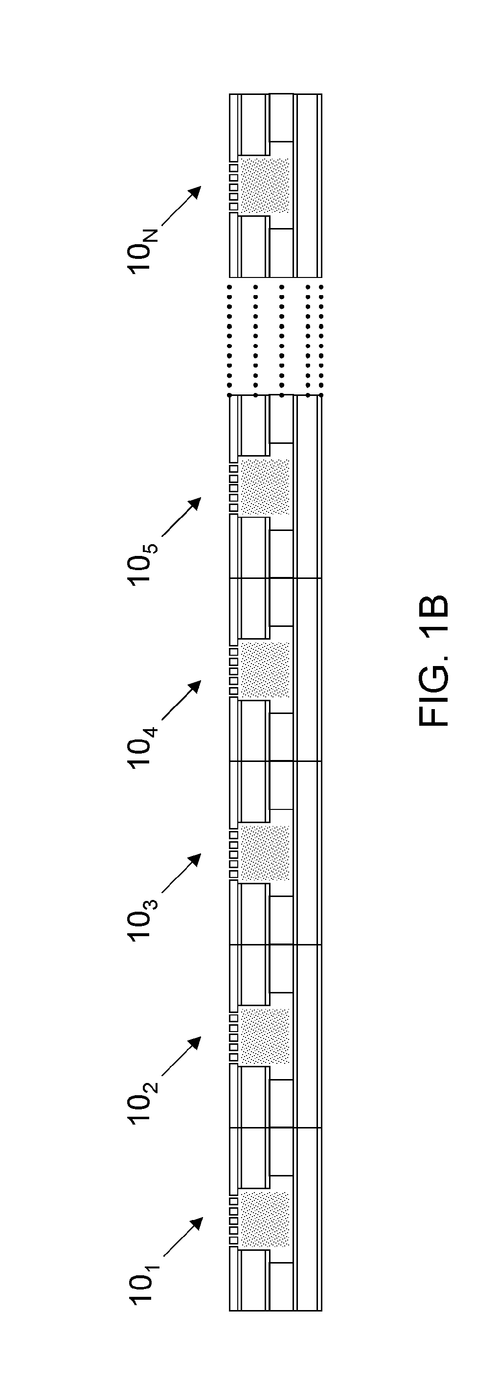
[0013]Microcavity plasma devices and arrays of the invention are modulated by a controllable electron emitter requiring a substantially smaller voltage than that applied across a microcavity in the device or array to generate a plasma. A driving voltage is applied across microcavity plasma devices while a small control voltage is applied to one or more electron emitters that inject electrons into the microcavity of a device. The effect of electron injection into a microplasma is to increase both the conductance current and light emitted by the plasma. While a voltage comparable to previous microcavity plasma devices is still imposed across the microcavity plasma devices, control of the devices can be accomplished at high speeds and with a small voltage, e.g., about 5V to 30V in preferred embodiments.

[0014]An embodiment of the invention is a microcavity plasma device that can be controlled by a low voltage electron emitter. The microcavity plasma device includes driving electrodes di...


PUM


Abstract

An embodiment of the invention is a microcavity plasma device that can be controlled by a low voltage electron emitter. The microcavity plasma device includes driving electrodes disposed proximate to a microcavity and arranged to contribute to generation of plasma in the microcavity upon application of a driving voltage. An electron emitter is arranged to emit electrons into the microcavity upon application of a control voltage. The electron emitter is an electron source having an insulator layer defining a tunneling region. The microplasma itself can serve as a second electrode necessary to energize the electron emitter. While a voltage comparable to previous microcavity plasma devices is still imposed across the microcavity plasma devices, control of the devices can be accomplished at high speeds and with a small voltage, e.g., about 5V to 30V in preferred embodiments.

Description

PRIORITY CLAIM AND REFERENCE TO RELATED APPLICATION[0001]This application claims priority under 35 U.S.C. §119 from prior provisional application Ser. No. 61 / 000,388, which was filed on Oct. 25, 2007.STATEMENT OF GOVERNMENT INTEREST[0002]This invention was made with government support under Contract No. F49620-03-1-0391 awarded by the U.S. Air Force Office of Scientific Research. The government has certain rights in the invention.FIELD[0003]A field of the invention is microcavity plasma devices (also known as microplasma devices) and arrays of microcavity plasma devices.BACKGROUND[0004]Microcavity plasma devices spatially confine a low temperature, nonequilibrium plasma to a cavity with a characteristic dimension d below 1 mm, and as small as 10 μm×10 μm. Researchers at the University of Illinois have developed and demonstrated a range of microcavity plasma devices and arrays of microcavity plasma devices. A number of fabrication processes and device structures have advanced the sta...

Claims


Application Information

Patent Timeline
IPC IPC(8): H05B41/36H01J17/48H01J17/49
CPCH01J61/82H01J11/18
Inventor EDEN, J. GARYCHEN, KUO-FENG
Owner THE BOARD OF TRUSTEES OF THE UNIV OF ILLINOIS
Why Eureka
Try Eureka