Laminated electronic component and manufacturing method therefor

Active Publication Date: 2010-11-18
MURATA MFG CO LTD
View PDF25 Cites 32 Cited by
  • Summary
  • Abstract
  • Description
  • Claims
  • Application Information

AI Technical Summary

Benefits of technology

[0026]According to preferred embodiments of the present invention, the water repellent is provided after the formation of the first plating layer and before the formation of the second plating layer. More specifically, when the first plating layer is provided to electrically connect the plurality of internal electrodes to each other and the second plating layer is provided to improve the laminated electronic component in terms of mounting property, the water repellent is applied before the formation of the plating layer for improving mounting property. Therefore, the highly corrosive complexing agent for use in a plating solution for, for example, tin plating or gold plating, in order to improve mounting property is prevented from entering the inside of the component main body, thereby allowing the reliability of the laminated electronic component to be sufficiently ensured.
[0027]Furthermore, since the water repellent is applied after the formation of the first plating layer, a thin water repellent film can be forme

Problems solved by technology

Thus, a plating solution entering the component main body along the interfaces between the internal electrodes and the insulator layers may erode the ceramic defining the insulator layers and the internal electrodes, thereby causing structural defects.
Furthermore, this causes defects in terms of reliability, such as degraded load characteristics against humidity for the laminated electronic component.

Method used


Image

  • Laminated electronic component and manufacturing method therefor
  • Laminated electronic component and manufacturing method therefor
  • Laminated electronic component and manufacturing method therefor

Examples


Example

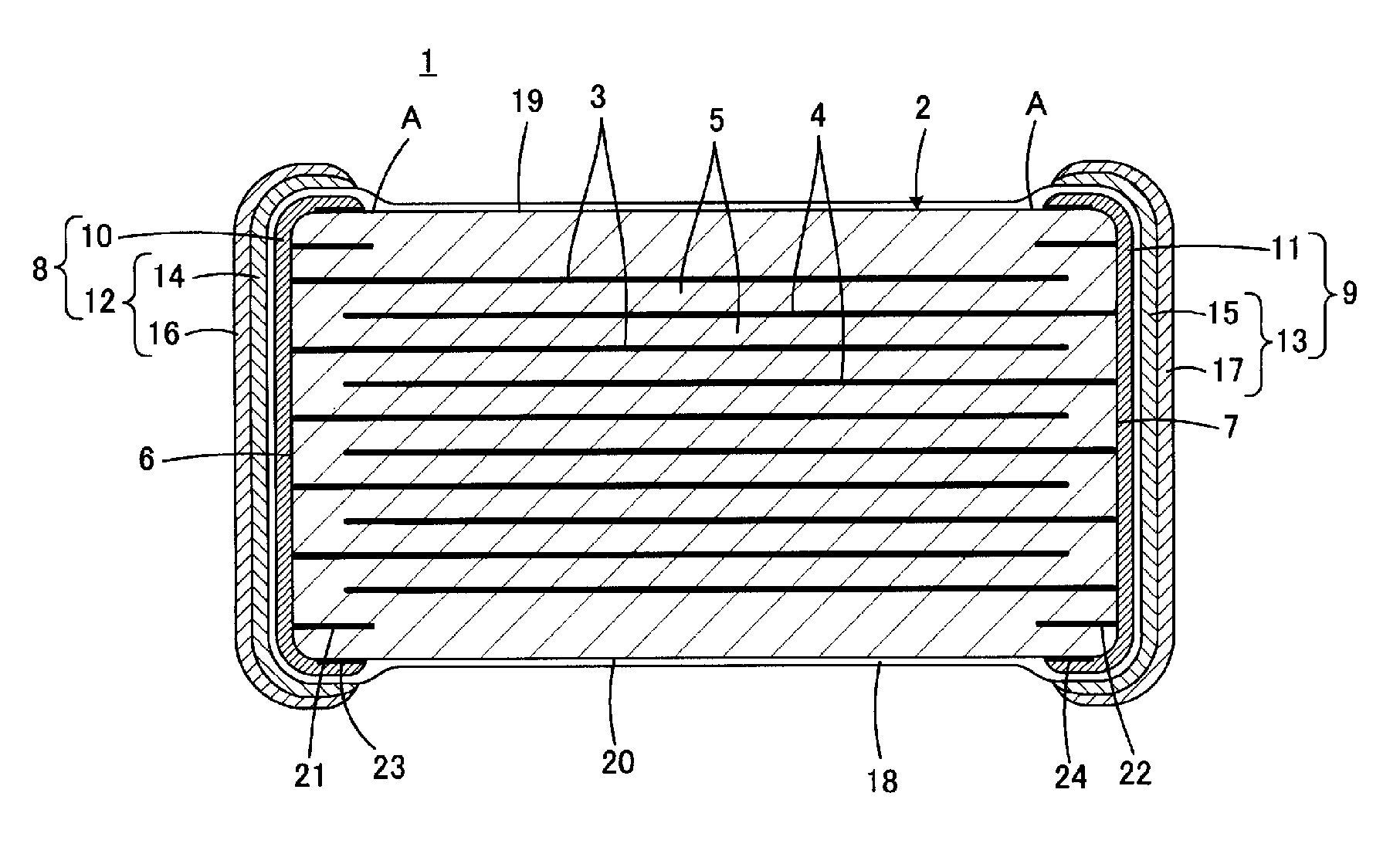
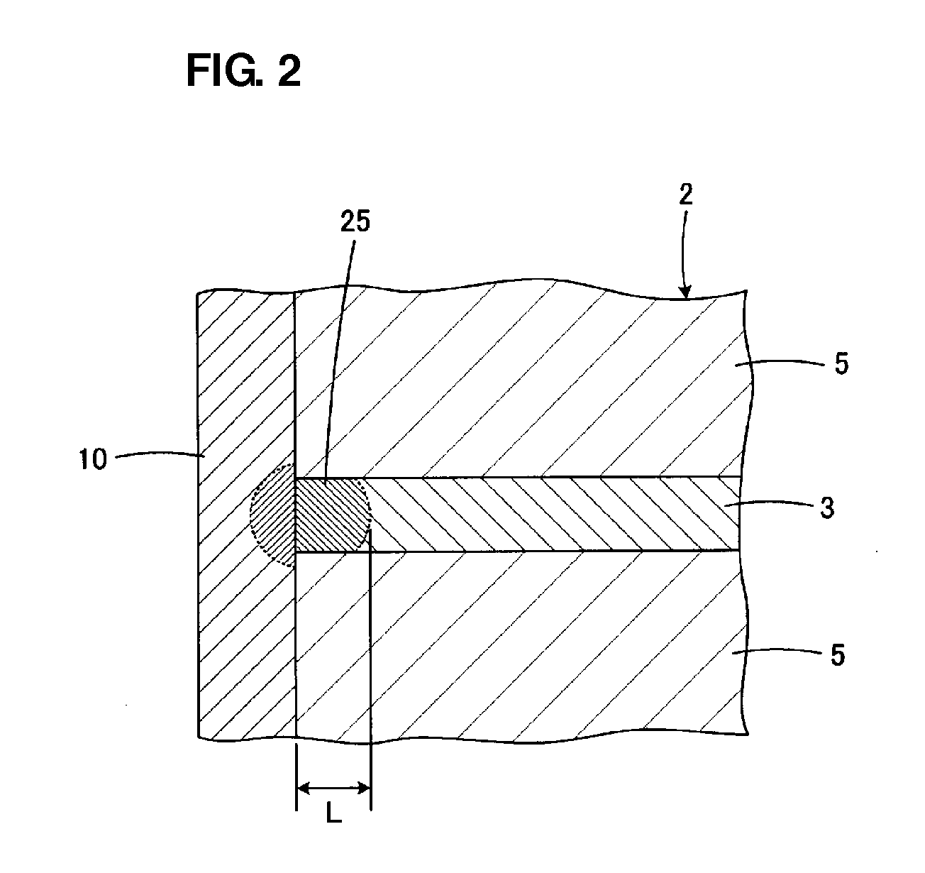
[0035]In a method for manufacturing a laminated electronic component according to preferred embodiments of the present invention, the formation of external terminal electrodes is based on the application of plating directly onto end surfaces of a component main body at which internal electrodes are exposed, without including the formation of a paste electrode, a sputtered electrode, a deposited electrode, or other similar electrode. Further, a plating film includes at least two layers, and typically, a first plating layer is provided to electrically connect a plurality of internal electrodes to each other, and a second plating layer is provided thereon to improve the mounting properties of the laminated electronic component. In the method according to a preferred embodiment of the present invention, after the formation of the first plating layer and before the formation of the second plating layer, a water repellent is applied at least to a surface of the first plating layer and to ...


PUM

PropertyMeasurementUnit
Lengthaaaaaaaaaa
Temperatureaaaaaaaaaa
Densityaaaaaaaaaa

Abstract

A method for manufacturing a laminated electronic component includes the steps of preparing a component main body having a laminated structure, the component main body including a plurality of internal electrodes formed therein, and each of the internal electrodes being partially exposed on an external surface of the component main body, and forming an external terminal electrode on the external surface of the component main body such that the external terminal electrode is electrically connected to the internal electrodes. The step of forming the external terminal electrode includes the steps of forming a first plating layer on exposed surfaces of the internal electrodes of the component main body, applying a water repellant at least on a surface of the first plating layer and on a section in the external surface of the component main body at which an end edge of the first plating layer is located, and then forming a second plating layer on the first plating layer having the water repellant applied thereon.

Description

BACKGROUND OF THE PRESENT INVENTION[0001]1. Field of the Present Invention[0002]The present invention relates to a laminated electronic component and a method for manufacturing the laminated electronic component, and more particularly, to a laminated electronic component with external terminal electrodes formed directly by plating so as to be electrically connected to a plurality of internal conductors, and to a method for manufacturing the laminated electronic component.[0003]2. Description of the Related Art[0004]As shown in FIG. 3, a laminated electronic component 101 typified by a laminated ceramic capacitor generally includes a component main body 105 having a laminated structure, which includes a plurality of laminated insulator layers 102 composed of, for example, a dielectric ceramic, and a plurality of layered internal electrodes 103 and 104 provided along interfaces between the adjacent insulator layers 102. Respective ends of the plurality of internal electrodes 103 and r...

Claims


Application Information

Patent Timeline
IPC IPC(8): H01G4/008H01G4/005H01G4/228H01G4/00H01G4/12H01G4/232H01G4/30
CPCH01G4/232H01G4/30H01G4/2325
Inventor MOTOKI, AKIHIROOGAWA, MAKOTOKAWASAKI, KENICHITAKEUCHI, SHUNSUKE
Owner MURATA MFG CO LTD
Why Eureka
Try Eureka