Plasma processing apparatus

a plasma processing and apparatus technology, applied in the field of microelectronics technologies, can solve the problems of difficult to adapt to the requirements of different technical processes, difficult to control the plasma energy and plasma density individually, and the inability to achieve the desirable effect of decoupling etc., and achieve the effect of improving the adaptability of the plasma processing apparatus

Inactive Publication Date: 2010-11-25
BEIJING NAURA MICROELECTRONICS EQUIP CO LTD
View PDF12 Cites 29 Cited by
  • Summary
  • Abstract
  • Description
  • Claims
  • Application Information

AI Technical Summary

Benefits of technology

[0021]An object of the present invention is to provide a plasma processing apparatus, in a reaction chamber of which plasma energy can be adjusted in a large range, so that many different technical process requirements can be satisfied.
[0032]As mentioned above, the technology described in the background art allows RF current to flow through the passive electrode or prevents RF current from flowing through the passive electrode, by changing the band pass of the filter circuit, so as to switch among different plasma energies.
[0033]Different from this, the plasma processing apparatus provided by the present invention applies a completely different idea to adjust the plasma energy in the reaction chamber. That is, the present invention changes current flowing through the passive electrode by adjusting impedance of the loop to which the passive electrode belongs (realized by adjusting the resistance of the impedance adjusting element), so as to change the plasma energy in the chamber reaction. The new idea provided by the present invention can adjust the magnitude of RF current in the passive electrode in a larger range. So, the plasma processing apparatus provided by the present invention overcomes the above mentioned shortcoming that the plasma energy can only be switched among some certain isolated values, and can realize more technical processes with different plasma density requirements in one and the same reaction chamber, so that adaptability of the plasma processing apparatus is improved greatly.

Problems solved by technology

However, due to the coupling between the first RF source 171 and the second RF source 172, it is difficult to control the plasma energy and the plasma density individually.
However, some drawbacks as follows exist in the plasma processing apparatus of the above mentioned technology.
Therefore, the desirable effect of decoupling of the plasma processing apparatus cannot be obtained.
It is more important that it is difficult for the plasma processing apparatus of the above mentioned technology to adjust the plasma energy effectively, so that it is difficult to adapt to requirements of different technical processes.
That is, such manner can only adjust the above effective area ratio between two isolated values.
Therefore, the plasma processing apparatus in the above technology can only satisfy requirements of a few technical processes and cannot adjust the plasma density in a large range.
The adaptability thereof thus is poor and cannot satisfy requirements of many technical processes.
So, problems that require the persons skilled in the art to solve now are how to effectively adjust the plasma density in the plasma processing apparatus so as to satisfy requirements of many technical processes, and how to achieve a more complete decoupling of different RF currents.

Method used


Image

  • Plasma processing apparatus
  • Plasma processing apparatus
  • Plasma processing apparatus

Examples


first embodiment

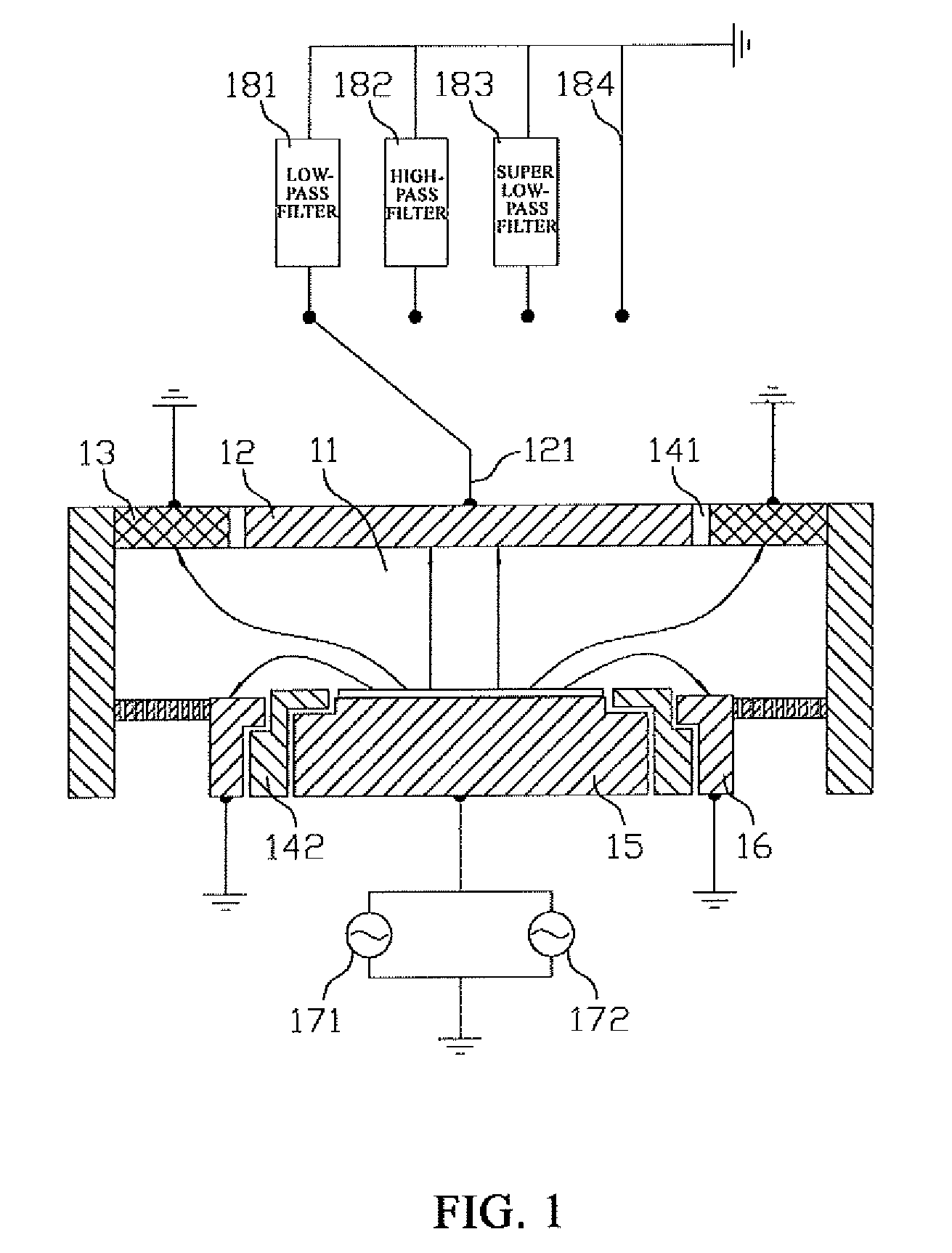
[0044]Reference is made to FIG. 2 which is a schematic view of a structure of a plasma processing apparatus according to the present invention.

[0045]In the first embodiment, the plasma processing apparatus provided by the present invention comprises a shell (for which no reference sign is shown), in which there is a reaction chamber 21.

[0046]A passive electrode 22 is provided on the top of the reaction chamber 21, and the passive electrode 22 is grounded via a first variable resistor R1 as a first impedance adjusting element. A first grounded ring 23 surrounds the passive electrode 22, and the first grounded ring 23 and the passive electrode 22 insulates from each other by a first insulating ring 241. Obviously, the first grounded ring 23 should be grounded.

[0047]Obviously, the first variable resistor R1 can be replaced by other impedance adjusting elements. For example, a resistor and a capacitor can be connected in series to act as the above mentioned first impedance adjusting ele...

second embodiment

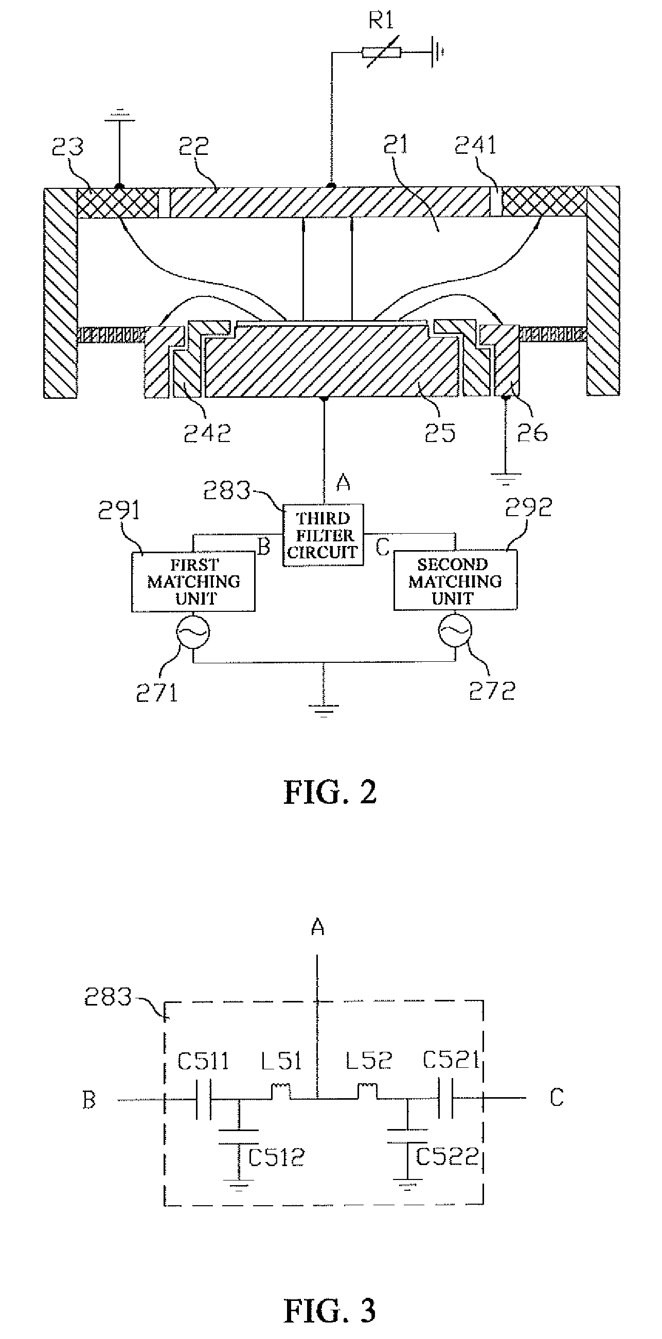
[0069]Reference is made to FIG. 4 which is a structural schematic diagram of a plasma processing apparatus according to the present invention.

[0070]In the second embodiment, the plasma processing apparatus provided by this embodiment is made a further improvement on the basis of the first embodiment.

[0071]As mentioned above, in order to widen the adaptability of the plasma processing apparatus, parameters associated with plasma in the reaction chamber 21 should be able to be adjusted. The parameters usually involve the plasma density, the plasma energy, the plasma flow etc. The adjustment of the plasma energy is usually carried out by the first RF source 271; the adjustment of the plasma density is usually carried out by the second RF source 272.

[0072]When the above parameters are adjusted in order to adapt to different technical processes, it is better to control the plasma density and the plasma energy separately. However, it is difficult to realize the separate control of the pla...

third embodiment

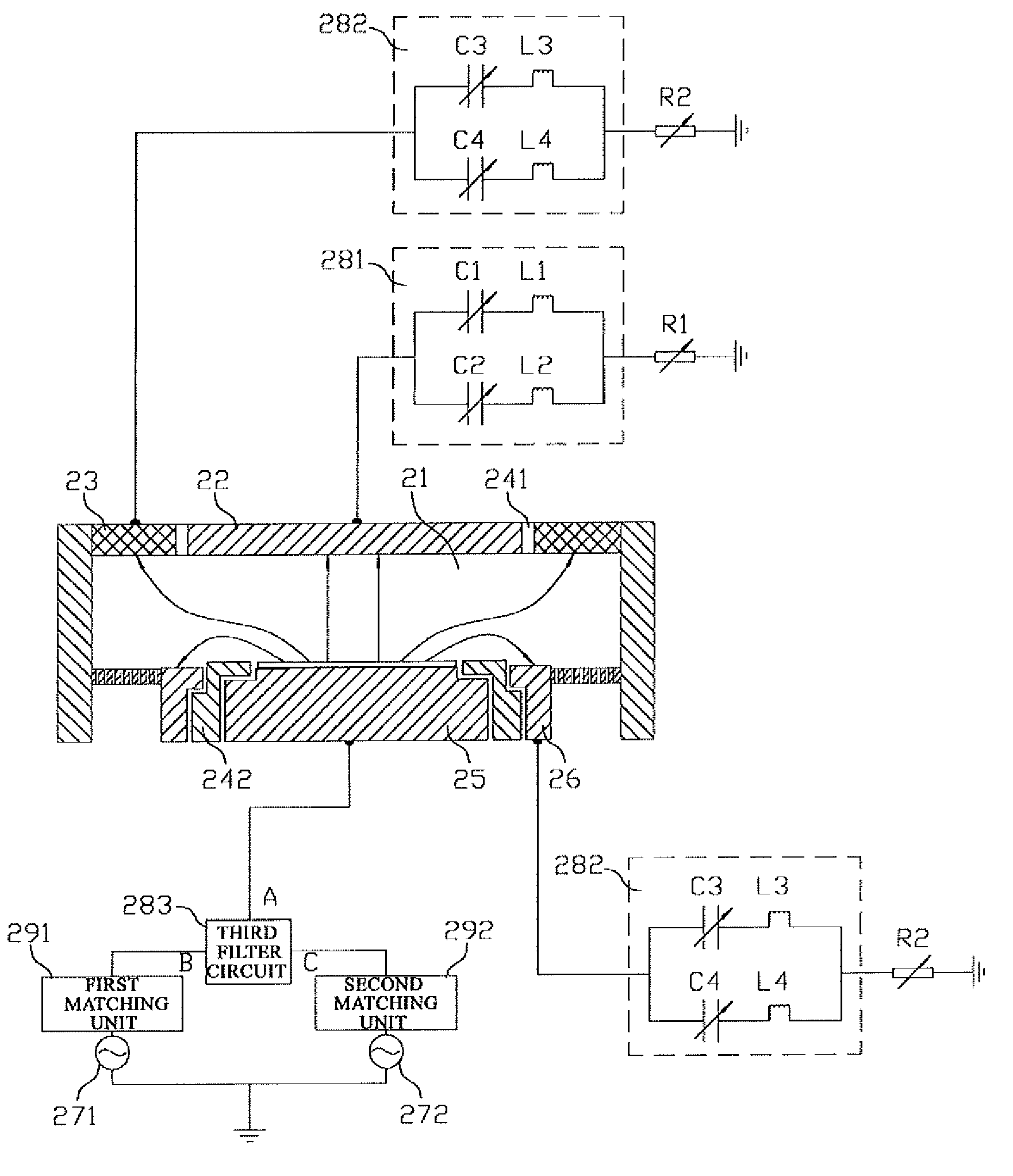
[0082]Now a reference is made to FIG. 5 which is a structural schematic diagram of a plasma processing apparatus according to the present invention.

[0083]In the third embodiment, the plasma processing apparatus provided by this embodiment is made an improvement on the basis of the first and second embodiments.

[0084]In the first and second embodiments, the first grounded ring 23 and the second grounded ring 26 both are grounded directly. In the instant embodiment, a second variable resistor R2 as a second impedance adjusting element can be connected in series between the first grounded ring 23 and the ground, and / or between the second grounded ring 26 and the ground.

[0085]Similar to the above mentioned first variable resistor R1, the second variable resistor R2 can also be replaced by other impedance adjusting elements. For example, a resistor and a capacitor connected in series can be used as the above second impedance adjusting element.

[0086]The second variable resistor R2 is furth...


PUM

PropertyMeasurementUnit
frequencyaaaaaaaaaa
frequencyaaaaaaaaaa
impedanceaaaaaaaaaa

Abstract

A plasma processing apparatus, comprising: a RF driving electrode (25) and a passive electrode (22) mounted face to face; a first grounded ring (23) surrounding the passive electrode (22) and insulated from it, a second grounded ring (26) surrounding the RF driving electrode (25) and insulated from it; the RF driving electrode (25) is connected with a first RF source (271) and a second RF source (272) respectively; a first impedance adjusting element is connected in series between the passive electrode (22) and the ground. The plasma processing apparatus overcomes a shortcoming that plasma energy can only be changed over among several certain isolated values, and thus technical processes with different plasma density requirements can be realized in one and the same reaction chamber.

Description

FIELD OF THE INVENTION[0001]The invention relates to the field of microelectronics technologies, especially to a plasma processing apparatus.BACKGROUND OF THE INVENTION[0002]A plasma processing apparatus is a processing equipment widely used in the semiconductor manufacturing field.[0003]Reference could be made to FIG. 1 which is a schematic diagram of a structure of a common plasma processing apparatus.[0004]The plasma processing apparatus usually comprises a shell (for which no reference sign is shown), in which there is a reaction chamber 11. The top of the reaction chamber 11 is provided with a passive electrode 12 and a top grounded ring 13 surrounding the passive electrode 12, which are insulated from each other by a first insulating ring 141. The bottom of the reaction chamber 11 is provided with a radio frequency (RF) driving electrode 15 and a bottom grounded ring 16 surrounding the RF driving electrode 15, which are insulated from each other by a second insulating ring 142...

Claims


Application Information

Patent Timeline
Patent Type & Authority Applications(United States)
IPC IPC(8): C23F1/08C23C16/00
CPCH01J37/32091H01J37/32174H01J37/32642H01J37/32623H01J37/32577
Inventor JIANHUI, NAN
Owner BEIJING NAURA MICROELECTRONICS EQUIP CO LTD
Why Eureka
Try Eureka