Level shift circuit
a level shift and circuit technology, applied in the direction of electrical equipment, pulse automatic control, baseband system details, etc., can solve the problems of large amount of power and require a complicated circuit, and achieve the effects of low power dissipation, high reliability, and high performan
- Summary
- Abstract
- Description
- Claims
- Application Information
AI Technical Summary
Benefits of technology
Problems solved by technology
Method used
Image
Examples
first embodiment
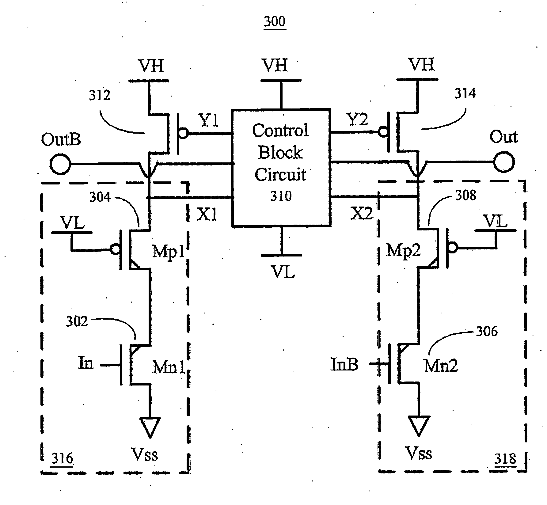
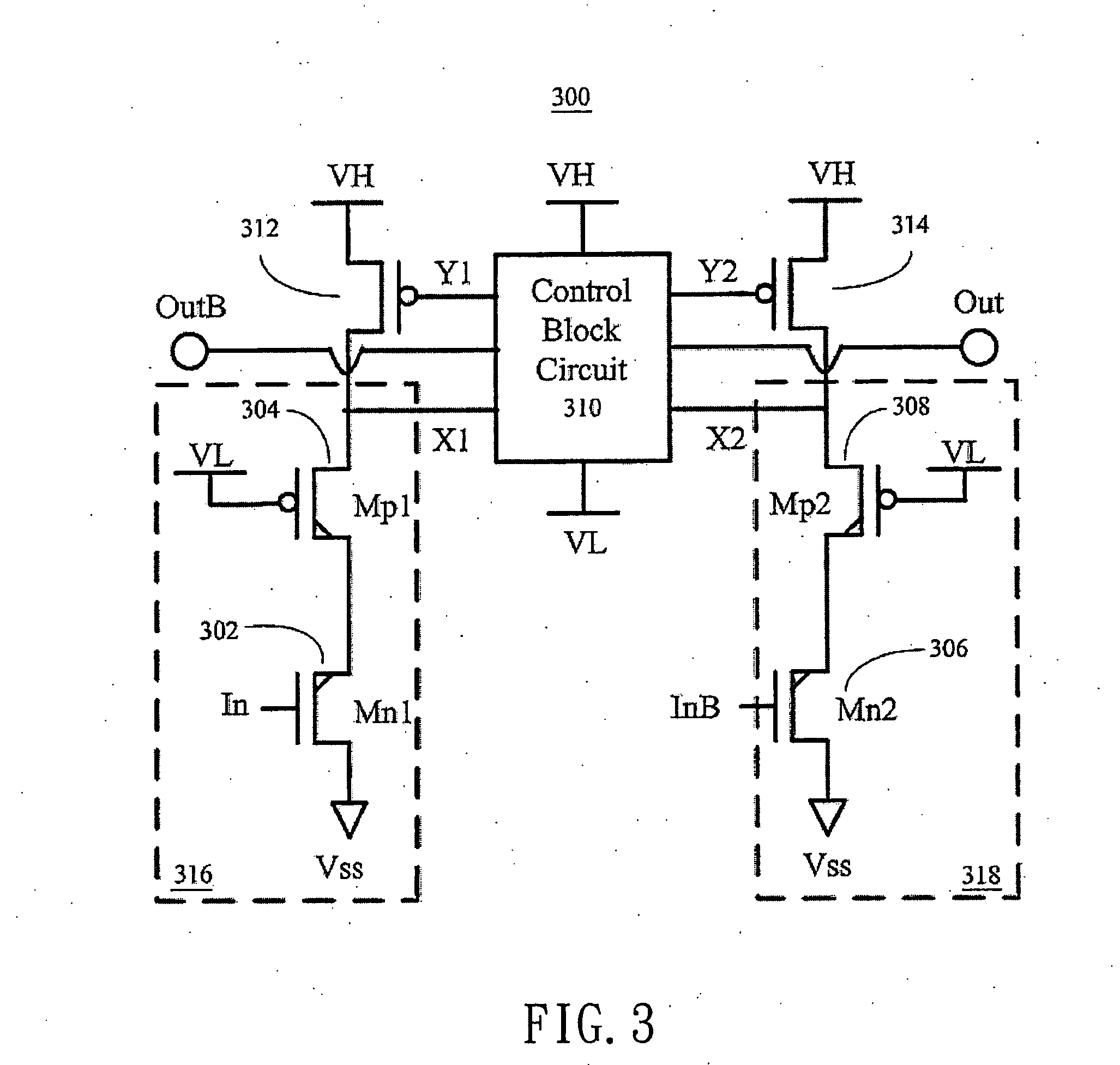
[0019]FIG. 3 is a circuit diagram of a level shift circuit 300 according to the present invention. The level shift circuit 300 comprises a first voltage level transfer unit 316, a second voltage level transfer unit 318, a control block circuit 310, a first PMOS pull-up transistor 312 and a second PMOS pull-up transistor 314. The first voltage level transfer unit 316 further comprises a NMOS transistor 302 and a PMOS transistor 304, wherein the gate of NMOS transistor 302 receives a first input signal which is operated in first voltage level (Vdd and Vss), the source of the NMOS transistor 302 is coupled to the supply voltage Vss, and the drain and gate of PMOS transistor 304 are respectively coupled to the NMOS transistor 302 and supply voltage VL for outputting the level transferred control signal X1 (operated in VH and VL level). On the other hand, the second voltage level transfer unit 318 comprises NMOS transistor 306 and PMOS transistor 308, wherein the gate of NMOS transistor ...
second embodiment
[0023]FIG. 6 is a circuit diagram of a level shift circuit 600 according to the present invention. The level shift circuit 600 comprises a first voltage level transfer unit 616, a second voltage level transfer unit 618, a control block circuit 610, a first NMOS pull-down transistor 612 and a second NMOS pull-down transistor 614. The first voltage level transfer unit 616 further comprises PMOS transistor 602 and NMOS transistor 604, wherein the gate of PMOS transistor 602 receives a first input signal which is operated in first voltage level (Vdd and Vss), the source of the PMOS transistor 602 is coupled to the supply voltage Vdd, and the drain and gate of NMOS transistor 604 are respectively coupled to the PMOS transistor 602 and supply voltage VH for outputting the level transferred control signal X1 (operated in VH and VL level). On the other hand, the second voltage level transfer unit 618 comprises PMOS transistor 606 and NMOS transistor 608, wherein the gate of PMOS transistor ...
PUM
 Abstract
Description
Claims
Application Information


