Field effect transistor fabrication from carbon nanotubes

a technology of carbon nanotubes and field effects, which is applied in the field of fabrication of devices including nanotubes, can solve the problems of affecting the ability to readily integrate them into advanced electronics, and the heat dissipation is becoming a critical problem

Active Publication Date: 2010-11-25
PURDUE RES FOUND INC
View PDF93 Cites 30 Cited by
  • Summary
  • Abstract
  • Description
  • Claims
  • Application Information

AI Technical Summary

Problems solved by technology

However, heat dissipation is becoming a critical problem with advanced electronic chips, and many researchers are looking for salvation to come from the integration of new nanomaterials into transistor technology.
However, several obstacles remain to be resolved in the growth and placement of CNTs, and these issues currently hinder the ability to readily integrate them into advanced electronics.

Method used


Image

  • Field effect transistor fabrication from carbon nanotubes
  • Field effect transistor fabrication from carbon nanotubes
  • Field effect transistor fabrication from carbon nanotubes

Examples


Embodiment Construction

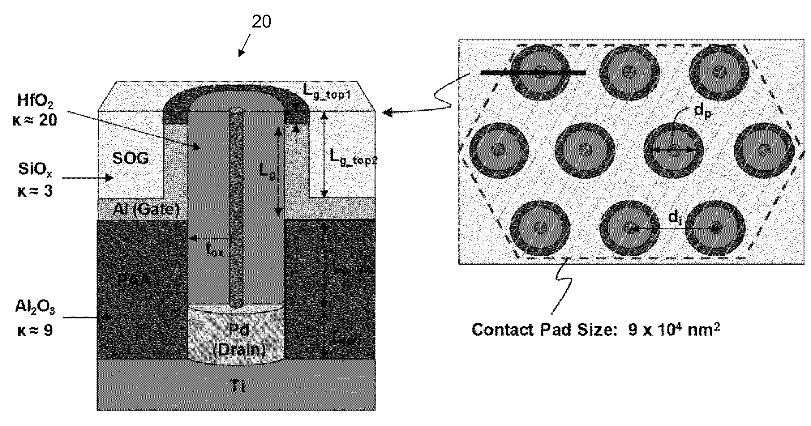
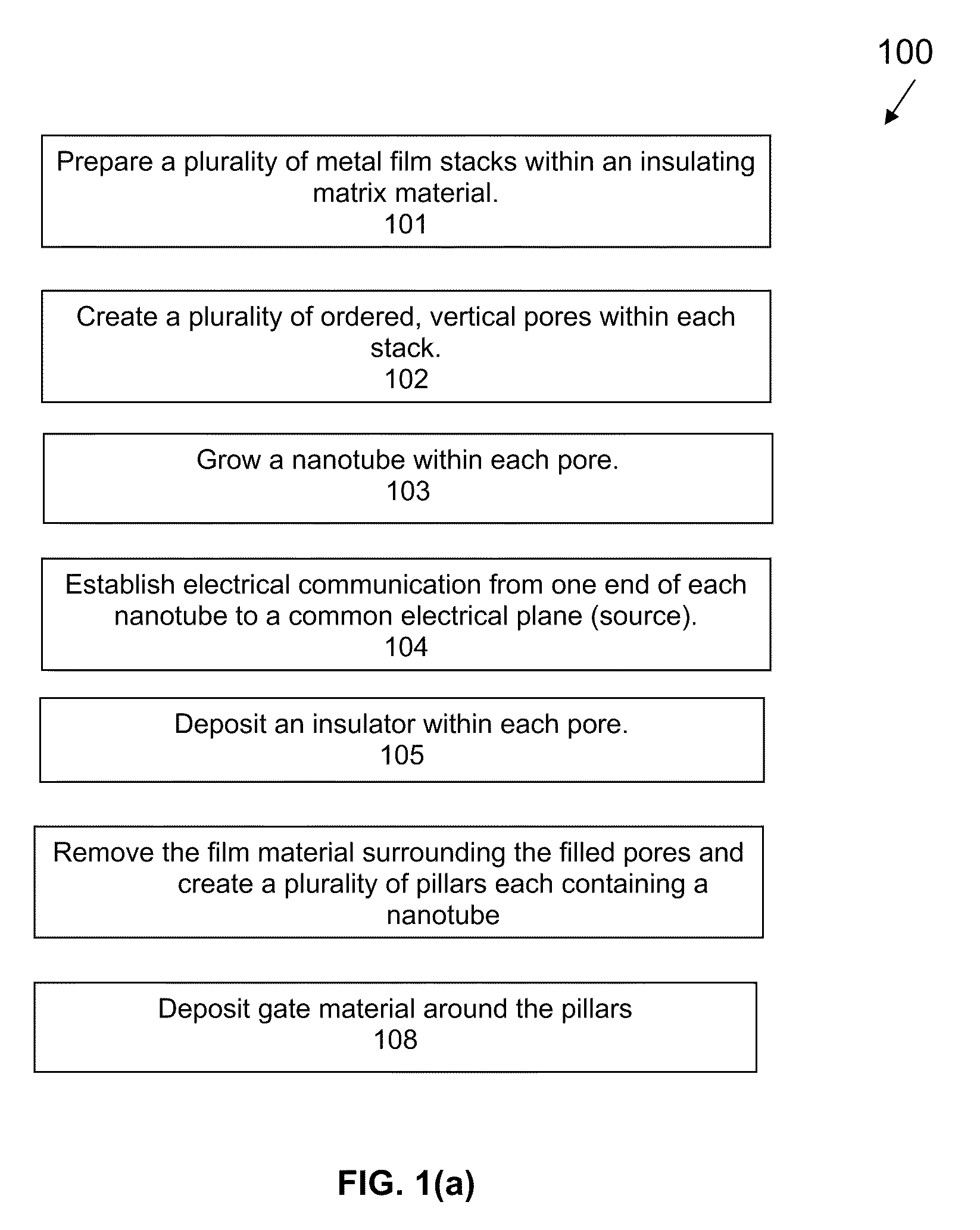
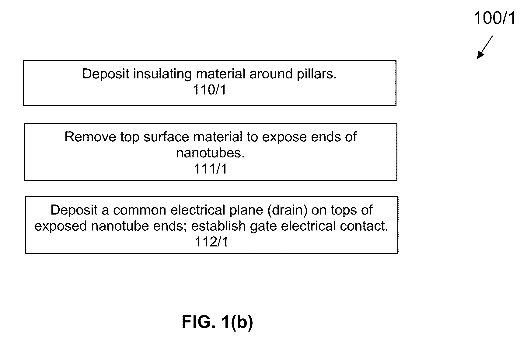
[0097]For the purposes of promoting an understanding of the principles of the invention, reference will now be made to the embodiments illustrated in the drawings and specific language will be used to describe the same. It will nevertheless be understood that no limitation of the scope of the invention is thereby intended, such alterations and further modifications in the illustrated device, and such further applications of the principles of the invention as illustrated therein being contemplated as would normally occur to one skilled in the art to which the invention relates. At least one embodiment of the present invention will be described and shown, and this application may show and / or describe other embodiments of the present invention. It is understood that any reference to “the invention” is a reference to an embodiment of a family of inventions, with no single embodiment including an apparatus, process, or composition that should be included in all embodiments, unless otherw...


PUM

PropertyMeasurementUnit
diameteraaaaaaaaaa
diameteraaaaaaaaaa
diameteraaaaaaaaaa

Abstract

Methods and apparatus for an electronic device such as a field effect transistor. One embodiment includes fabrication of an FET utilizing single walled carbon nanotubes as the semiconducting material. In one embodiment, the FETs are vertical arrangements of SWCNTs, and in some embodiments prepared within porous anodic alumina (PAA). Various embodiments pertain to different methods for fabricating the drains, sources, and gates.

Description

CROSS REFERENCE TO RELATED APPLICATION[0001]This application claims the benefit of priority to U.S. Provisional Patent Application Ser. No. 61 / 166,953, filed Apr. 6, 2009, entitled FABRICATION OF FIELD EFFECT TRANSISTORS FROM CARBON NANOTUBES, incorporated herein by reference.FIELD OF THE INVENTION[0002]Various embodiments of the present invention pertain to the fabrication of devices including nanotubes, and in particular to electronic devices including semiconducting carbon nanotubes.BACKGROUND OF THE INVENTION[0003]With a market that constantly hungers for smaller, faster, and cheaper electronics, the ability for Si transistor technology to continue to satisfy the demands will soon reach its end. Marvelous innovations, such as strained Si, have enabled engineers to continue to shrink Si transistors while maintaining reasonable device performance. However, heat dissipation is becoming a critical problem with advanced electronic chips, and many researchers are looking for salvation...

Claims


Application Information

Patent Timeline
Patent Type & Authority Applications(United States)
IPC IPC(8): H01L29/775H01L21/77H01L21/336H01L21/20H01L29/78
CPCB82Y10/00H01L29/0665H01L51/057H01L51/0508H01L51/0048H01L23/373H01L2924/0002H10K85/221H10K10/46H10K10/491H01L2924/00
Inventor FRANKLIN, AARON D.SANDS, TIMOTHY D.FISHER, TIMOTHY S.JANES, DAVID B.
Owner PURDUE RES FOUND INC
Why Eureka
Try Eureka