Semiconductor device and method for manufacturing the same

a semiconductor device and manufacturing method technology, applied in the field of semiconductor devices, can solve problems such as deteriorating the yield and reliability of semiconductor devices

Inactive Publication Date: 2010-11-25
PANASONIC CORP
View PDF11 Cites 14 Cited by
  • Summary
  • Abstract
  • Description
  • Claims
  • Application Information

AI Technical Summary

Benefits of technology

[0027]Here, in the step (d), the second barrier metal film may be removed so that an upper end of the second barrier metal film on the side surface of the wiring groove is lower than an upper end of the side surface of the wiring groove. Thereby, an elution of Cu in the wiring groove due to the battery effect can be prevented more reliably because the second barrier metal film is not exposed to a polished surface during CMP for the films containing copper.
[0028]Moreover, a standard electrode potential of the first barrier metal film is equal to or lower than that of copper, and a standard electrode potential of the second barrier metal film is higher than that of copper. Thereby, an elution of Cu due to the battery effect can also be prevented during CMP for the barrier metal films.
[0029]Furthermore, in the step (c), the second barrier metal film can also be formed discontinuously. Thereby, it is possible to provide an effect that a corrosion of copper is even harder to occur because a contact area between the second barrier metal film and slurry is small.

Problems solved by technology

The elution of the Cu film is a significant problem of deteriorating a yield and a reliability of a semiconductor device.

Method used


Image

  • Semiconductor device and method for manufacturing the same
  • Semiconductor device and method for manufacturing the same
  • Semiconductor device and method for manufacturing the same

Examples


first embodiment

(First Embodiment)

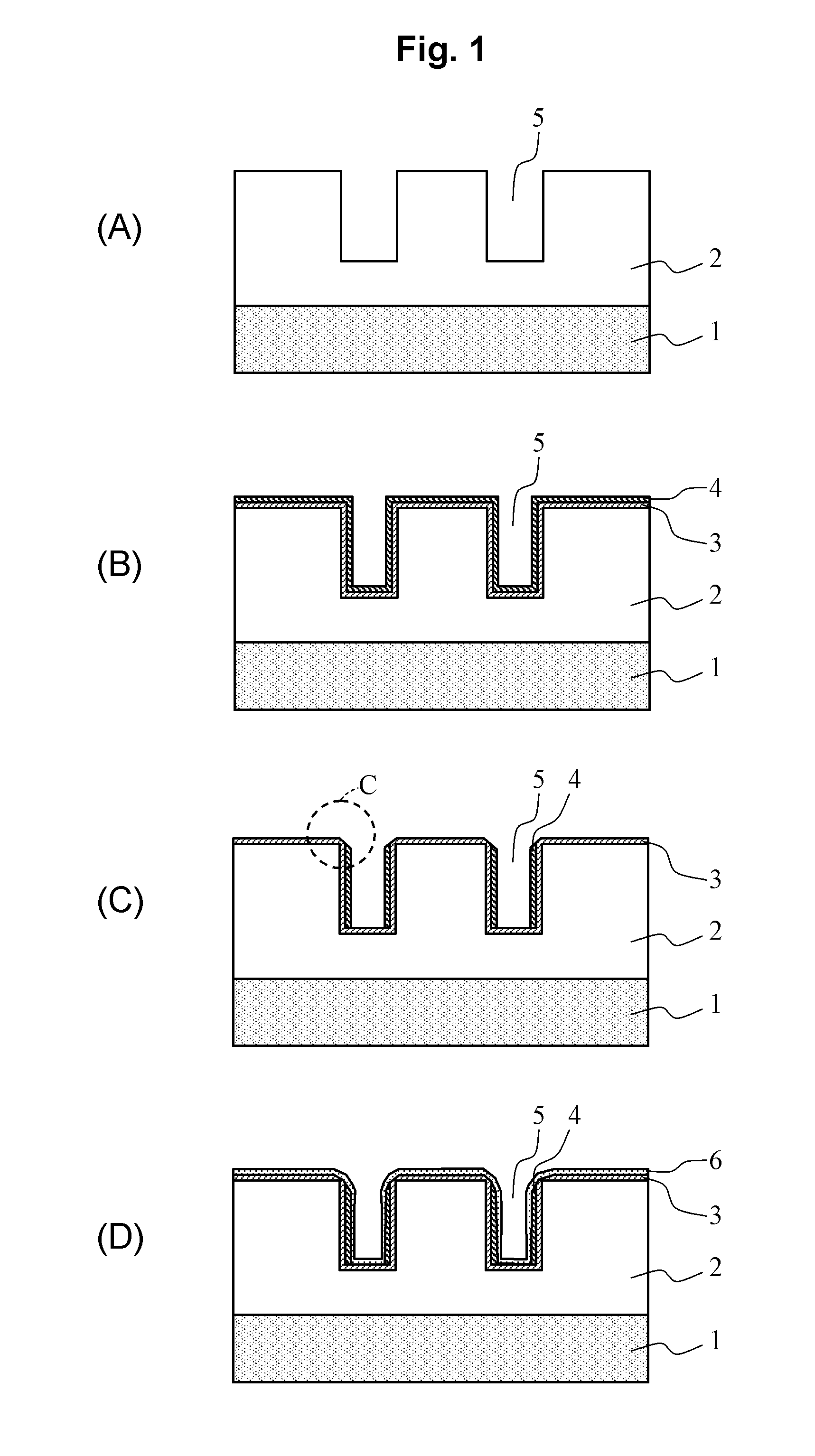
[0044]A manufacturing method in a first embodiment relating to the present invention is described by using FIGS. 1A to 1D and 2A to 2C.

[0045]First, as shown in FIG. 1A, a first interlayer insulating film 2 is formed on a semiconductor substrate 1 in a film thickness of 250 nm, and then a wiring groove 5 is formed in the first interlayer insulating film 2 by conventional lithographic technique and dry etching technique. The wiring groove 5 is connected to a semiconductor element, a capacitance element, a resistance element, and so on formed on the semiconductor substrate 1 to form an LSI (Large Scale Integrated Circuit) although they are omitted in the figure. A device of 32 nm node or finer is supposed, and a width of the wiring groove 5 is 50 nm or less. Here, an insulting film with a low dielectric constant, e.g., an SiOC film or a porous SiOC film having pores in the film or the like can be used as a material of the first interlayer insulating film 2.

[0046]Next,...

second embodiment

(Second Embodiment)

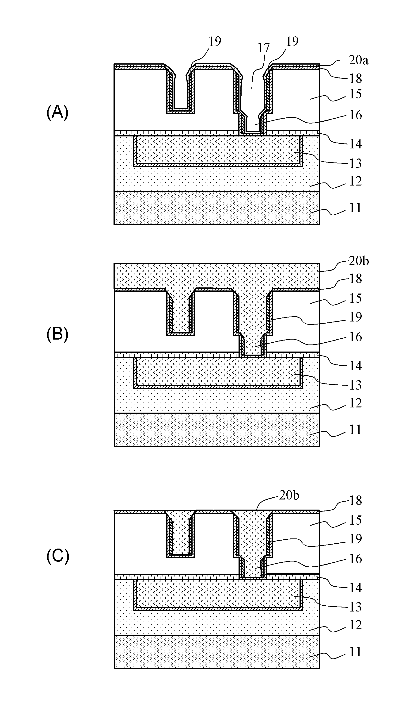
[0061]A manufacturing method of a semiconductor device in a second embodiment relating to the present invention is described with reference to FIGS. 3A to 3C, 4A to 4C, and 5A to 5C.

[0062]First, as shown in FIG. 3A, a first interlayer insulating film 12 is formed on a semiconductor substrate 11 in a film thickness of 250 nm, and then a first Cu wiring 13 is formed in the first interlayer insulating film 12. Then, a liner film 14 is formed on the first interlayer insulating film 12 and the first Cu wiring 13. Then, a second interlayer insulating film 15 is formed on the liner film 14. Subsequently, in the liner film 14 and the second interlayer insulating film 15, a via hole 16 reaching the first Cu wiring 13 and a wiring groove 17 for forming a second Cu wiring are formed. Here, an SiOC film or a porous SiOC film or the like can be used as materials for the first interlayer insulating film 12 and the second interlayer insulating film 15 as in the first embodiment....

third embodiment

(Third Embodiment)

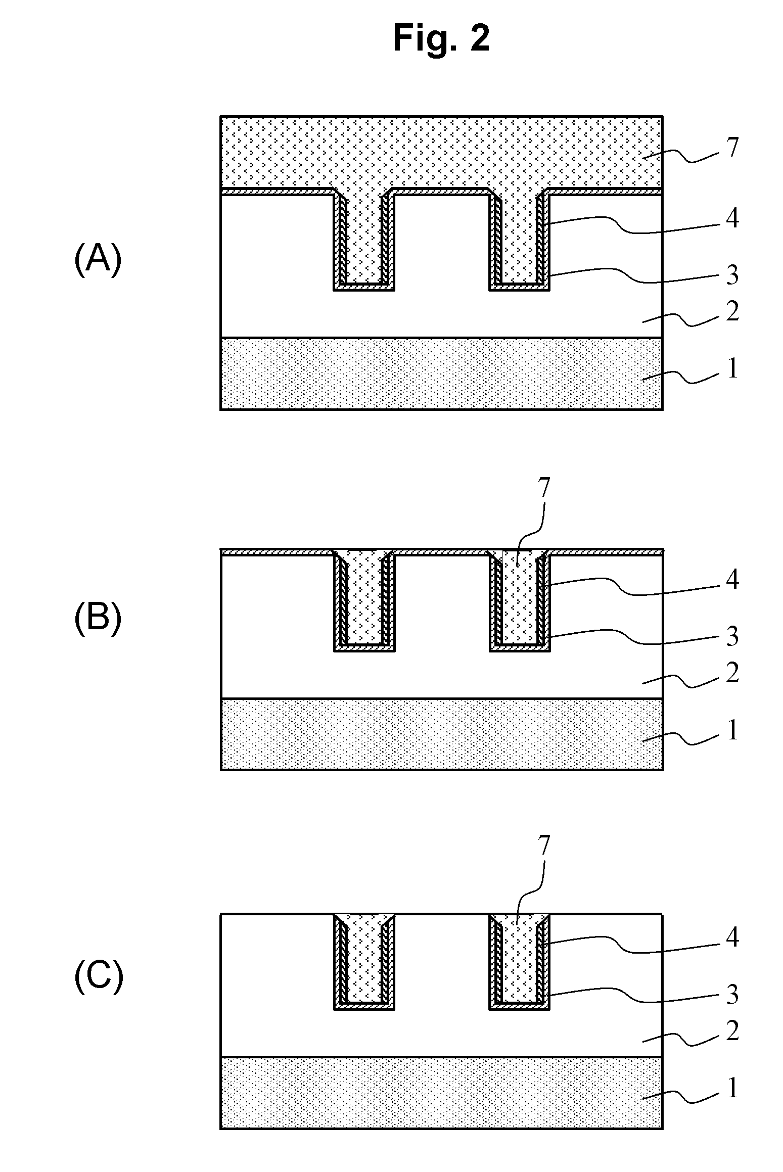
[0075]Although a case of forming the second barrier metal films 4, 19 so as to be continuous films in the first and second embodiments has been described, a case of forming these films 4, 19 so as to be discontinuous films will be described with reference to FIGS. 6A to 6D, 7A, and 7B. As a method of forming a discontinuous film, there is a method wherein a supply of a process gas is stopped before a forming film is to be a continuous film.

[0076]As shown in FIG. 6A, first, a first interlayer insulating film 2 is formed on a semiconductor substrate 1 in a film thickness of 250 nm, and then a wiring groove 5 is formed in the first interlayer insulating film 2. This is the same as the first embodiment.

[0077]Next, as shown in FIG. 6B, a first barrier metal (TaN) film 3 is formed on the first interlayer insulating film 2 including a side surface and a bottom surface of the wiring groove 5, and then a discontinuous film 26 which is a group of deposited Ru parts scattered...


PUM

PropertyMeasurementUnit
widthaaaaaaaaaa
widthaaaaaaaaaa
standard electrode potentialaaaaaaaaaa

Abstract

Provided is a method for forming a Cu wiring that does not cause Cu elution during CMP when a Ru material is used as a barrier metal film for the Cu wiring. The method has a step (d) of removing a second barrier metal film (Ru film) formed on a first barrier metal film on an upper surface of an interlayer insulating film, and a step (e) of depositing a seed copper (Cu) film on the first and the second barrier metal films after the step (d). By removing the second barrier metal film on the upper surface before the seed copper film is formed, copper is prevented from eluding into a slurry due to a battery effect of the second barrier metal film and copper.

Description

CROSS-REFERENCE TO RELATED APPLICATION[0001]This is a continuation of International Application No. PCT / JP2009 / 000551 filed on Feb. 12, 2009, which claims priority to Japanese Patent Application No. 2008-034185 filed on Feb. 15, 2008. The disclosures of these applications including specifications, drawings and claims are incorporated herein by reference in their entireties.BACKGROUND OF THE INVENTION[0002]1. Field of the Invention[0003]The present invention relates to a semiconductor device having a highly reliable wiring and, specifically, relates to a micro-pattern filling in a technique for forming embedded wiring.[0004]2. Description of the Related Art[0005]Recently, copper (Cu) having a lower resistance than aluminum and a high electromigration (EM) immunity has attracted attention as a wiring material for realizing high integration and high speed operation of a semiconductor integrated circuit. Dry etching of Cu material is difficult, therefore a wiring manufacturing method wh...

Claims


Application Information

Patent Timeline
Patent Type & Authority Applications(United States)
IPC IPC(8): H01L23/522H01L21/768
CPCH01L21/7684H01L21/76843H01L21/76844H01L21/76868H01L21/76873H01L23/53238H01L2924/0002H01L23/53295H01L2221/1089H01L2924/00
Inventor HIRAO, SHUJIKANEYAMA, SYUTETSU
Owner PANASONIC CORP
Why Eureka
Try Eureka