
Laminated electronic component and manufacturing method therefor

a technology of laminated electronic components and manufacturing methods, applied in the direction of capacitor details, coatings, capacitors, etc., can solve the problems of deformation of load characteristics, structural defects, reliability defects, etc., and achieve the effect of reducing the risk of failure, reducing the cost of manufacturing, and improving the quality of manufacturing

Active Publication Date: 2010-12-02
MURATA MFG CO LTD
View PDF28 Cites 63 Cited by
  • Summary
  • Abstract
  • Description
  • Claims
  • Application Information

AI Technical Summary

Benefits of technology

[0069]Next, non-limiting experimental examples will be described, which were performed to confirm the advantageous effects of the present invention.

Problems solved by technology

Thus, a plating solution entering the component main body along the interfaces between the internal electrodes and the insulator layers may erode the ceramic defining the insulator layers and the internal electrodes, thereby causing structural defects.
Furthermore, this results in defects in terms of reliability, such as degraded load characteristics against humidity for the laminated electronic component.
In particular, when tin or gold plating is to be applied, the problems described above are more likely to occur because a tin or gold plating solution generally contains a highly corrosive complexing agent.
However, such a heat treatment will cause the water repellent to disappear.
However, for example, when a treatment for providing strong water repellency is performed after the formation of the conductive resin layers, plating adhesion onto the conductive resin layers will be deteriorated, and problems such as no plating adhesion will be likely to occur.
WO2008 / 023496, rather than by baking, this problem will become more serious because the use of a water repellent with strong water repellency is desired.

Method used


Image

  • Laminated electronic component and manufacturing method therefor
  • Laminated electronic component and manufacturing method therefor
  • Laminated electronic component and manufacturing method therefor

Examples


Embodiment Construction

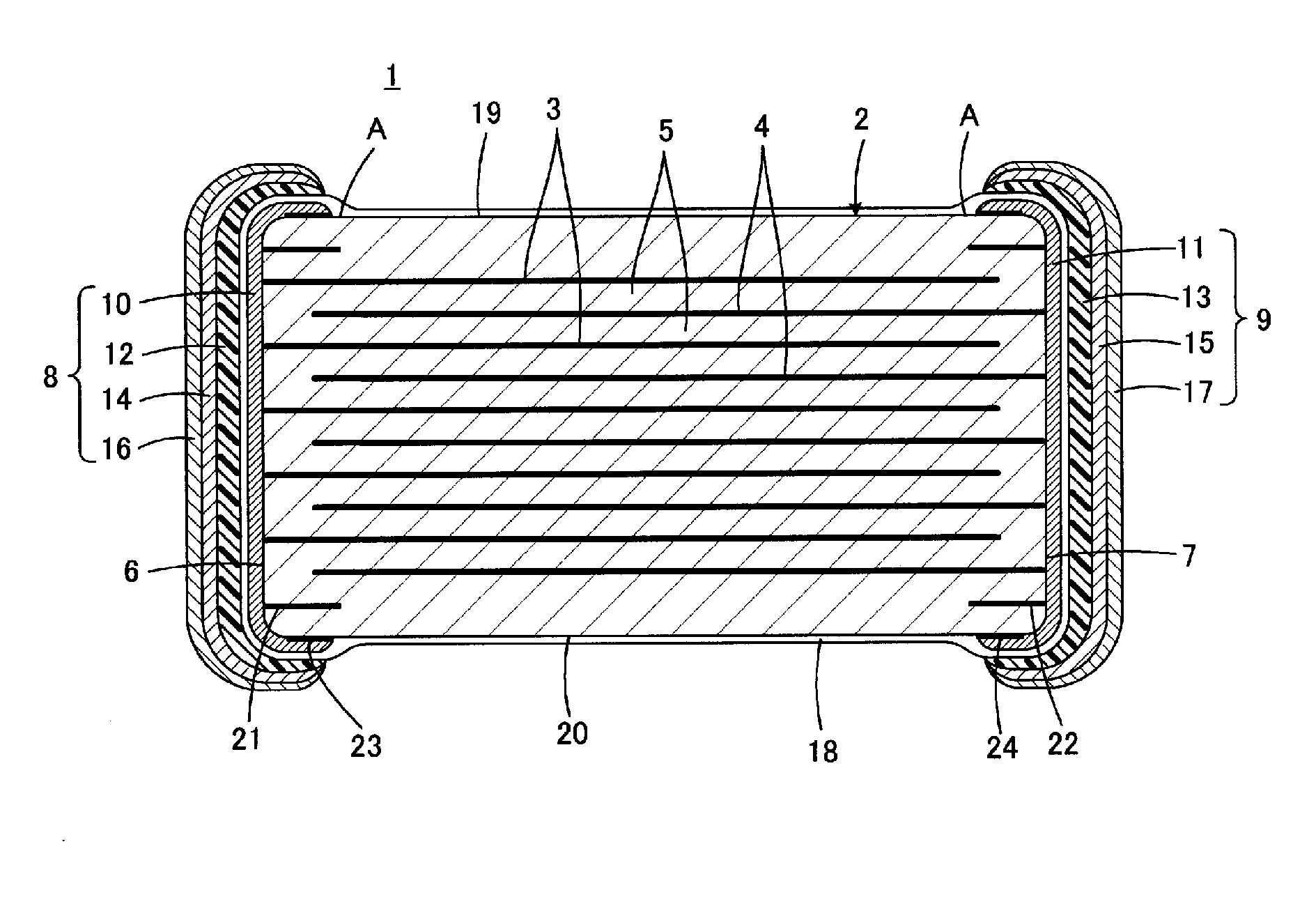
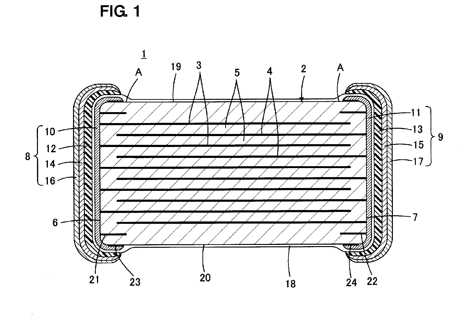
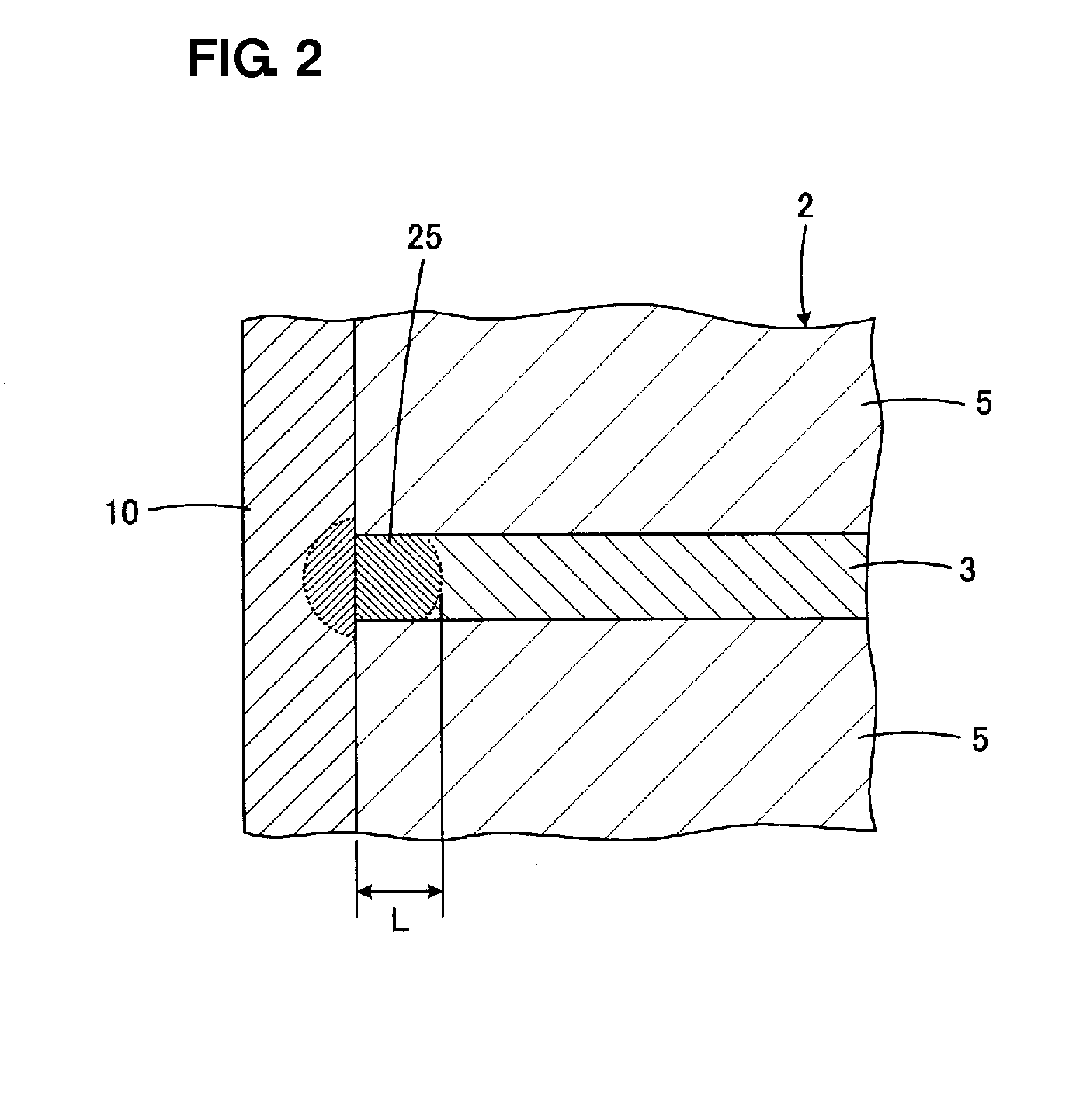
[0039]With reference to FIG. 1, a laminated electronic component 1 includes a component main body 2 having a laminated structure. The component main body 2 includes a plurality of internal electrodes 3 and 4 provided therein. More specifically, the component main body 2 includes a plurality of laminated insulator layers 5, and a plurality of layered internal electrodes 3 and 4 provided along interfaces between the adjacent insulator layers 5.

[0040]When the laminated electronic component 1 defines a laminated ceramic capacitor, the insulator layers 5 are preferably composed of a dielectric ceramic. It is to be noted that the laminated electronic component 1 may define a different element, such as an inductor, a thermistor, or a piezoelectric component, for example. Therefore, depending on the function of the laminated electronic component 1, the insulator layers 5 may be composed of a dielectric ceramic, or alternatively, a magnetic ceramic, a semiconductor ceramic, or a piezoelectri...


PUM


Abstract

A method for manufacturing a laminated electronic component includes the steps of preparing a component main body having a laminated structure, the component main body including a plurality of internal electrodes formed therein, and each of the internal electrodes being partially exposed on an external surface of the component main body, and forming an external terminal electrode on the external surface of the component main body such that the external terminal electrode is electrically connected to the internal electrodes. The step of forming the external terminal electrode includes the steps of forming a metal layer on exposed surfaces of the internal electrodes of the component main body, applying a water repellant on at least a surface of the metal layer and on a section of the external surface of the component main body at which an end edge of the metal layer is located, and then forming a conductive resin layer on the metal layer having the water repellant applied thereon.

Description

BACKGROUND OF THE PRESENT INVENTION[0001]1. Field of the Present Invention[0002]The present invention relates to a laminated electronic component and a method for manufacturing the laminated electronic component, and more particularly, to a structure of an external terminal electrode and a method for forming the external terminal electrode.[0003]2. Description of the Related Art[0004]As shown in FIG. 3, a laminated electronic component 101 typified by a laminated ceramic capacitor generally includes a component main body 105 having a laminated structure, which includes a plurality of laminated insulator layers 102 composed of, for example, a dielectric ceramic, and a plurality of layered internal electrodes 103 and 104 formed along interfaces between the adjacent insulator layers 102. Respective ends of the plurality of internal electrodes 103 and respective ends of the plurality of internal electrodes 104 are exposed at one end surface and the other end surface 106 and 107 of the c...

Claims


Application Information

Patent Timeline
IPC IPC(8): H01G4/228B05D5/12
CPCH01G4/2325H01G4/30
Inventor OGAWA, MAKOTOMOTOKI, AKIHIROSARUBAN, MASAHITOIWANAGA, TOSHIYUKITAKEUCHI, SHUNSUKEKAWASAKI, KENICHI
Owner MURATA MFG CO LTD
Features
  • Generate Ideas
  • Intellectual Property
  • Life Sciences
  • Materials
  • Tech Scout
  • Unparalleled Data Quality
  • Higher Quality Content
  • 60% Fewer Hallucinations
Learn More