
Method for producing plasma display panel

a plasma display and plasma technology, applied in the manufacture of electric discharge tubes/lamps, electrodes, electromechanical systems, etc., can solve the problems of difficult dispersion of phosphor into ink, insufficient emission properties of pdp, and phosphor degradation, so as to achieve efficient production of high-definition pdp and prevent phosphor degradation

Inactive Publication Date: 2010-12-02
PANASONIC CORP
View PDF7 Cites 0 Cited by
  • Summary
  • Abstract
  • Description
  • Claims
  • Application Information

AI Technical Summary

Benefits of technology

[0008]The present invention has been achieved to solve these problems, and it is an object of the present invention to provide a method for producing a PDP whereby luminance degradation of a phosphor can be prevented and a high definition PDP can be produced efficiently.
[0013]According to the present invention, degradation of luminance of a phosphor is prevented by using a phosphor having an average particle diameter of not less than 1.0 μm, and a high definition PDP can be produced efficiently.

Problems solved by technology

When the phosphor is crushed, it is considered that the luminance may degrade and thus the emission properties of a PDP can be insufficient.
Furthermore, a phosphor having a small particle size agglomerates easily, and this causes a problem in that the dispersion of the phosphor into an ink is difficult.
In the meantime, when discharge cells are arranged more finely for higher definition along with higher pixel counts of a plasma display panel, it becomes difficult to apply a phosphor ink to each discharge cell.
However, in order to form a phosphor layer having a predetermined thickness in each discharge cell, it is required to increase the number of cycles of applying a phosphor ink by an inkjet device and drying it, resulting in low productivity.

Method used


Image

  • Method for producing plasma display panel
  • Method for producing plasma display panel
  • Method for producing plasma display panel

Examples


first embodiment

(Structure of PDP)

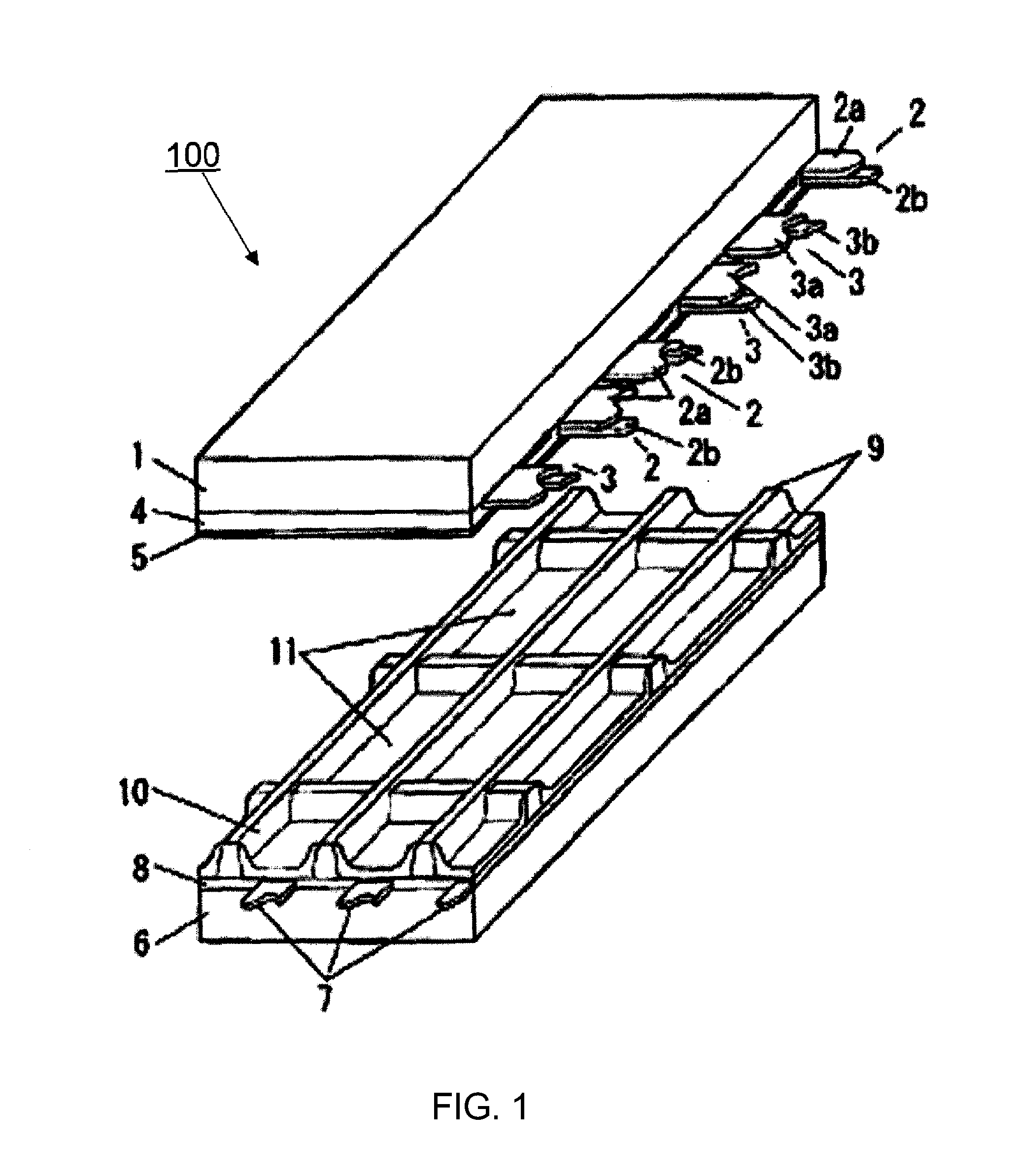
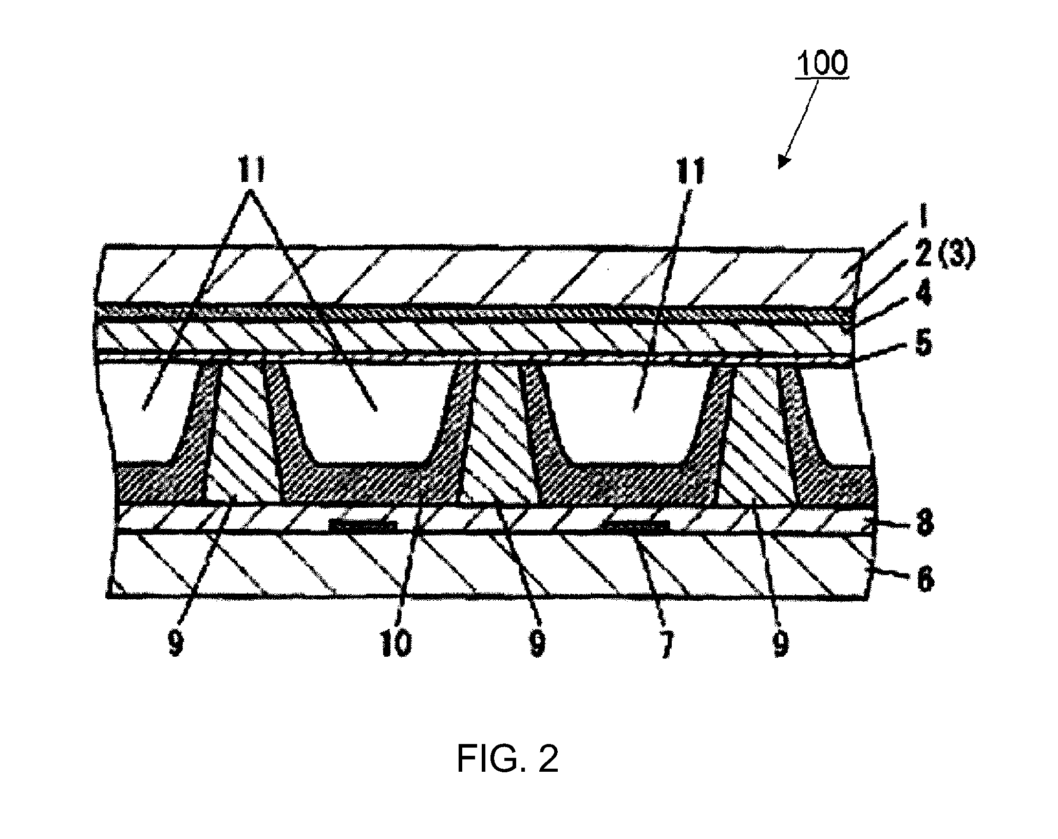
[0019]First, a general structure of a PDP to be produced is described. FIG. 1 is an exploded perspective view showing a structure of a PDP 100 in the first embodiment of the present invention, and FIG. 2 is a sectional view of a main portion of a discharge cell.

[0020]As shown in FIG. 1, the PDP 100 includes a front panel and a back panel with these panels being arranged facing each other. A lot of discharge cells 11 are formed between the front panel and the back panel.

[0021]The front panel includes a front substrate 1, scan electrodes 2, sustain electrodes 3, a dielectric layer 4, and a protective layer 5. The front substrate 1 is made of glass. A display electrode is composed of a pair of the scan electrode 2 and the sustain electrode 3, and a plurality of the display electrodes are formed parallel on the front substrate 1. The scan electrodes 2 and the sustain electrodes 3 are formed in the pattern in which an arrangement of a scan electrode 2—a sustain electrod...

second embodiment

[0039]Next, the second embodiment of the present invention will be described. The second embodiment differs from the first embodiment only in that each phosphor ink is different. Hence, only the phosphor inks will be described.

[0040]In the second embodiment, the phosphor ink is free from a binder made of a resin such as ethyl cellulose. In the second embodiment, the each phosphor ink has a good storage property. When a phosphor ink containing a binder made of a resin is stored sitting still, the phosphor particles settle with time, and precipitate on the bottom of a storage vessel of the phosphor ink. When the phosphor ink is left in this state, the phosphor particles may be bound by the resin component. However, the binder made of a resin is not added to the phosphor ink in this embodiment, and therefore, the phosphor particles is not bound even though the phosphor particles settle out during storage. The phosphor that has settled out in the each phosphor ink can be dispersed in th...

embodiment

Feature of Embodiment

[0048]Features of the above embodiments will be listed below. It should be noted that the present invention is not limited to the below features.[0049][C1] A method for producing a plasma display panel includes[0050]a step of providing a back substrate with a barrier rib (e.g., barrier rib 9) to form a plurality of recesses (e.g., discharge cells 11) separated each other by the barrier rib, and[0051]a step of applying a phosphor ink to the recesses using an inkjet device,

[0052]wherein the phosphor ink contains a phosphor having an average particle diameter of not less than 1.0 μm, a solvent and a dispersant, and the content of the phosphor in the phosphor ink is not less than 30 wt % and not more than 70 wt %.

[0053]According to the method, a phosphor ink containing a phosphor having sufficient luminance can be applied efficiently using an inkjet device, and thus a high definition PDP can be produced efficiently.[0054][C2] In one preferred embodiment of the metho...


PUM


Abstract

The present invention provides a method for producing a plasma display panel, including a step of providing a back substrate with a barrier rib to form a plurality of recesses separated each other by the barrier rib, and a step of applying a phosphor ink to the recesses using an inkjet device, wherein the phosphor ink contains a phosphor having an average particle diameter of not less than 1.0 μm, a solvent and a dispersant, and the content of the phosphor in the phosphor ink is not less than 30 wt % and not more than 70 wt %.

Description

BACKGROUND OF THE INVENTION[0001]1. Field of the Invention[0002]The present invention relates to a method for producing a plasma display panel that is used for image display, particularly to a method for producing the plasma display panel using an inkjet device.[0003]2. Description of Related Art[0004]In recent years, a plasma display panel (hereinafter, abbreviated as PDP) has attracted attention as a color display device that can achieve a large but thin screen with a light weight.[0005]In the PDP, image display is performed by making use of light emission from phosphor layers. For forming a phosphor layer in a production of a PDP, inkjet techniques have been proposed (e.g., see JP-A-2004-63246). Specifically, JP-A-2004-63246 discloses a method wherein an ink in which a phosphor having an average particle diameter of not less than 0.001 μm and less than 1.0 μm is dispersed in an organic solvent is prepared and then ejected from an end of an inkjet head.[0006]However, in order to u...

Claims


Application Information

Patent Timeline
Patent Type & Authority Applications(United States)
IPC IPC(8): H01J9/227H01J11/12H01J11/22H01J11/24H01J11/26H01J11/34H01J11/42
CPCH01J9/227H01J11/12H01J11/42
Inventor HASEGAWA, KENJINASU, SHOUGOSATO, KENJININOMIYA, SYOUZOUOOHATA, HISAYO
Owner PANASONIC CORP
Learn More