Through Silicon Via With Embedded Decoupling Capacitor

a decoupling capacitor and silicon via technology, applied in capacitors, semiconductor devices, semiconductor/solid-state device details, etc., can solve the problems of long response time, damage to the ics, and rapid power load change,

Active Publication Date: 2010-12-09
QUALCOMM INC
View PDF15 Cites 95 Cited by
  • Summary
  • Abstract
  • Description
  • Claims
  • Application Information

AI Technical Summary

Problems solved by technology

Only tenths of a volt lower may create erratic results in the ICs; only tenths of a volt higher may damage the ICs.
As transistors in the ICs turn on and off, the power load changes rapidly placing additional demand on the voltage regulator.
The distance between the voltage regulator and the ICs creates a long response time, preventing the voltage regulator from increasing power to the ICs instantaneously,

Method used


Image

  • Through Silicon Via With Embedded Decoupling Capacitor
  • Through Silicon Via With Embedded Decoupling Capacitor
  • Through Silicon Via With Embedded Decoupling Capacitor

Examples


Embodiment Construction

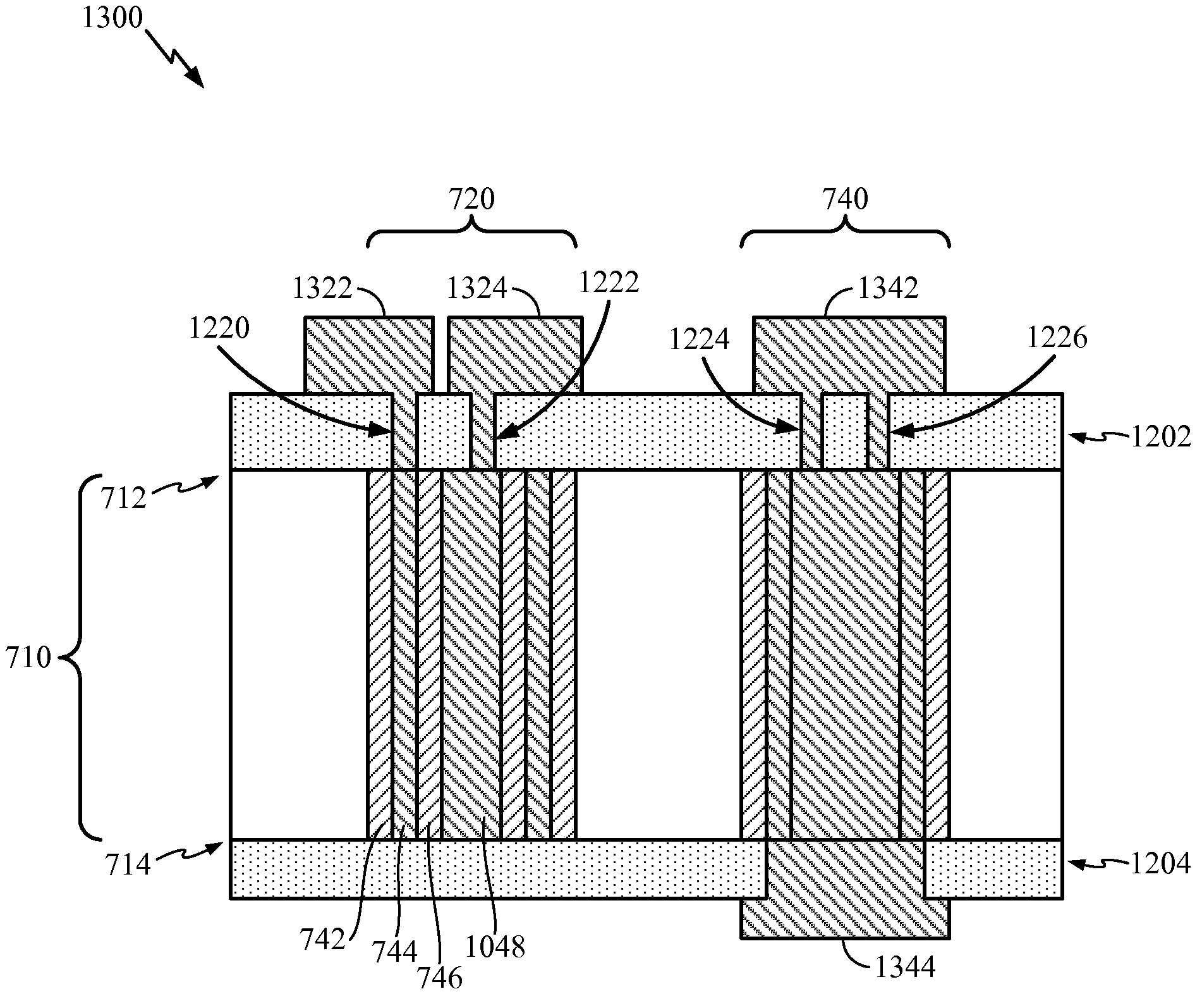
[0040]One method for providing decoupling of ICs from the die is to build the decoupling capacitors into the through silicon vias. Through silicon vias are already well integrated into the manufacturing process for stacked ICs, and large numbers exist on stacked ICs. Building decoupling capacitors into the through silicon vias has several advantages.

[0041]Removing conventional separate decoupling capacitors from the substrate increases the die area available for active circuitry. The reduction in die size leads to smaller portable electronic devices. Additionally, building the decoupling capacitor into a structure that is already present in the die reduces manufacturing costs. Fewer processes are used to embed the decoupling capacitor in through silicon vias than to build a separate decoupling capacitor.

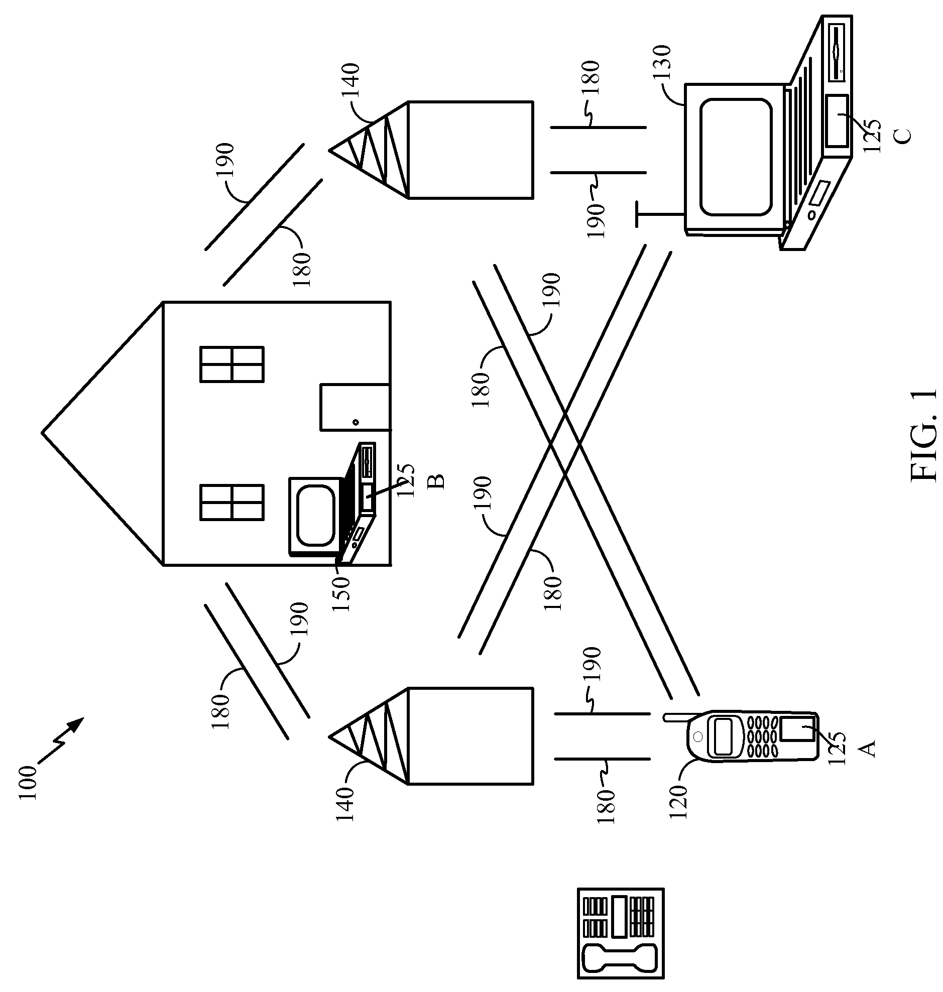
[0042]In FIG. 1, remote unit 120 is shown as a mobile telephone, remote unit 130 is shown as a portable computer, and remote unit 150 is shown as a fixed location remote unit in a wi...


PUM


Abstract

A semiconductor die, having a substrate, includes a through silicon via. The through silicon via includes a decoupling capacitor having a first co-axial conductor, a second co-axial conductor, and a co-axial dielectric separating the first co-axial conductor from the second co-axial conductor. The decoupling capacitor is configured to provide local charge storage for components on the semiconductor die.

Description

TECHNICAL FIELD[0001]The present disclosure generally relates to integrated circuits (ICs). More specifically, the present disclosure relates to decoupling circuitry for ICs.BACKGROUND[0002]ICs are generally fabricated on one side of a semiconductor die. These dies are then used to power a diverse range of electronics products. IC packages conventionally include only one layer of ICs. Building multiple layers of ICs (or “stacking” the ICs) in the same semiconductor package can significantly reduce the lateral size of electronics and reduce the cost of manufacturing. As a result, stacked ICs are quickly gaining popularity for further extending the capabilities of electronics.[0003]One feature used in building stacked ICs are through silicon vias (TSV). Through silicon vias are connections through the substrate of the die and may be used to connect a layer of ICs on one side of the substrate to an opposite side of the substrate where contacts may be provided for packaging the substrat...

Claims


Application Information

Patent Timeline
IPC IPC(8): H01L29/92H01L21/02
CPCH01L21/76898H01L23/481H01L2924/0002H01L2924/00014H01L2225/06541H01L23/642H01L25/0657H01L28/60H01L2223/6616H01L2223/6622H01L2224/0557H01L2224/06181H01L2225/06527H01L2224/05552
Inventor NOWAK, MATTHEW MICHAELGU, SHIQUN
Owner QUALCOMM INC
Why Eureka
Try Eureka