Driver circuit

a technology of driver circuit and driver, which is applied in the direction of pulse manipulation, pulse technique, emergency protective arrangement for limiting excess voltage/current, etc., can solve the problems of slow operation of high-withstand-voltage transistors, inability to meet high-speed operation, and inability to operate high-withstand-voltage transistors. to achieve the effect of preventing an overvoltag

Active Publication Date: 2010-12-09
RENESAS ELECTRONICS CORP
View PDF3 Cites 25 Cited by
  • Summary
  • Abstract
  • Description
  • Claims
  • Application Information

AI Technical Summary

Benefits of technology

[0035]In the configuration like this, since the first and second switch are provided, it is possible to prevent an overvoltage from being applied to the driver circuit by the On / Off control of the first and second switch. Further, by controlling the On / Off order of the first and second switch by using the overvoltage protection sequence circuit, the overvoltage is prevented from being applied to the driver circuit, in particular to the main-driver in any combination states of the On / Off states of the first and second power supplies and the enable mode / power-down modes. Therefore, the circuit can be protected from being destroyed by an overvoltage. Since the circuit is protected from an overvoltage in this way, it becomes possible to set the second power supply to a higher voltage and to form the main-driver by low-withstand-voltage (high-speed) transistors. As a result, the main-driver can be operated at a high speed with a large amplitude.

Problems solved by technology

However, it poses a problem that the demand for the high-speed operation cannot be satisfied.
However, in general, high-withstand-voltage transistors are slow in operation, whereas low-withstand-voltage transistors are fast in operation.
In particular, a voltage higher than the withstand-voltage tends to be applied to the gate-drain voltage Vgd, and thus often leading to the destruction of such transistors.
Therefore, there is a problem that the driver circuit 900 of FIG. 8 cannot perform a high-speed operation.

Method used


Image

  • Driver circuit
  • Driver circuit
  • Driver circuit

Examples


first exemplary embodiment

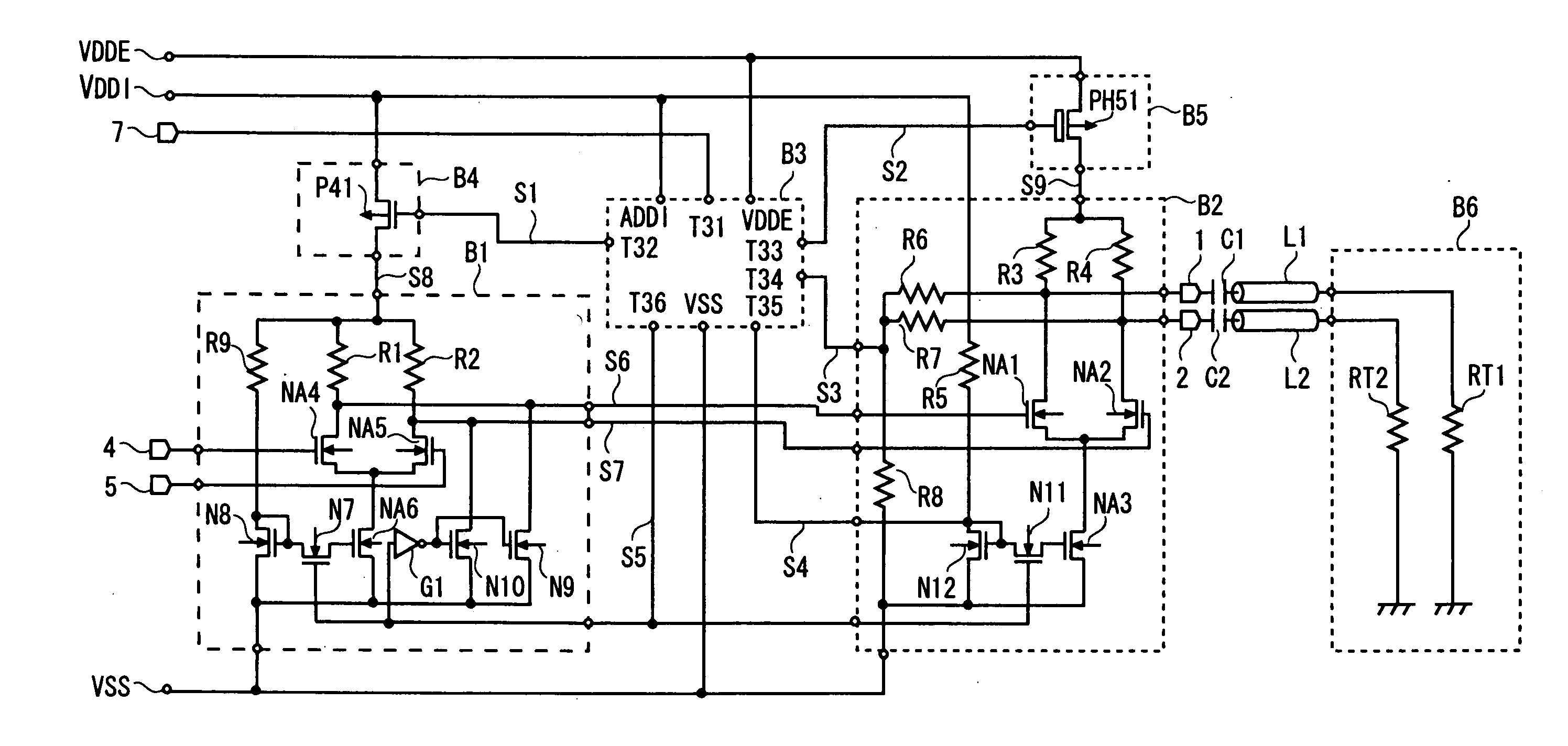
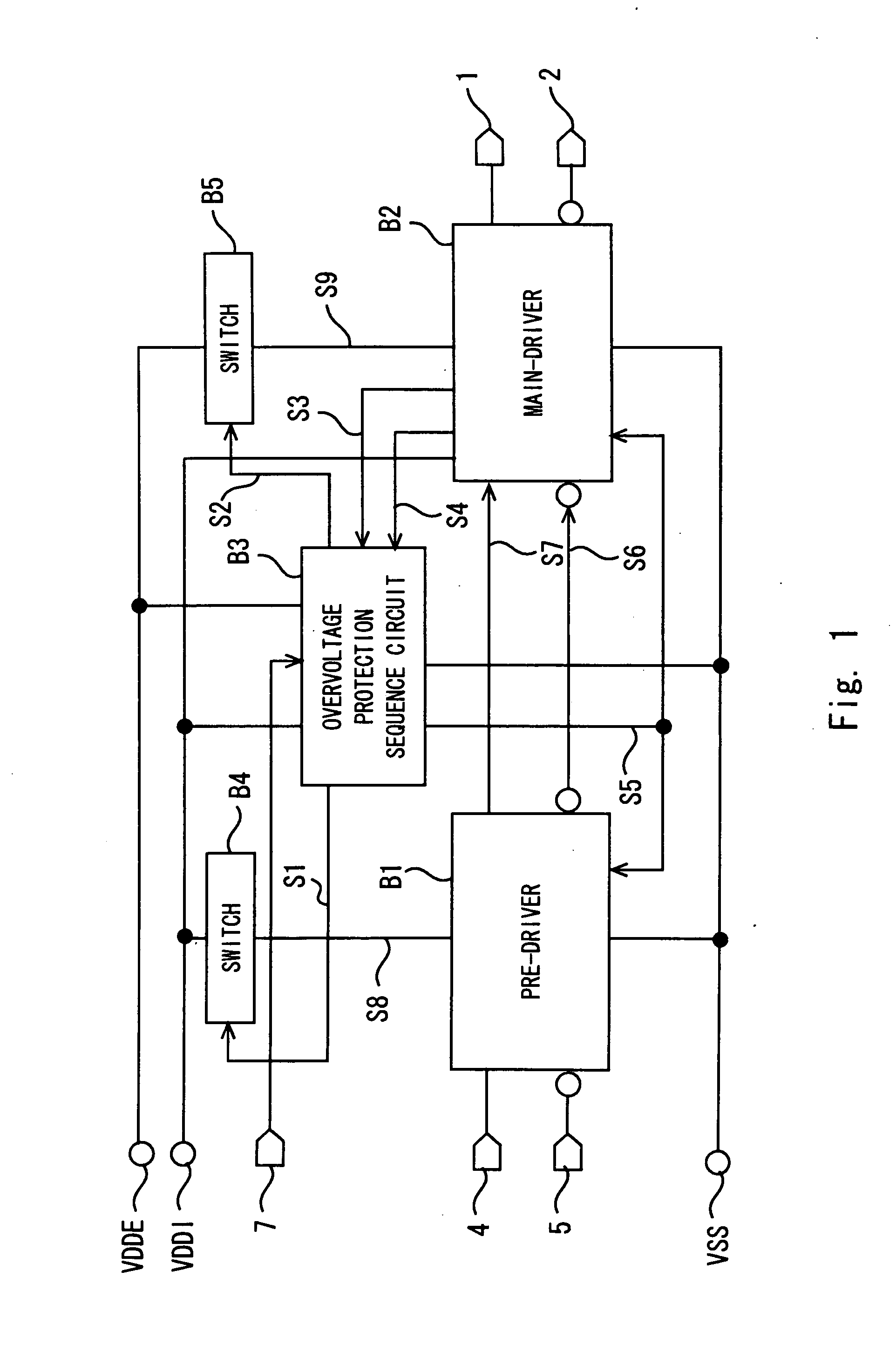
[0047]FIG. 1 is a functional block diagram of a first exemplary embodiment in accordance with a driver circuit of the present invention. In this first exemplary embodiment, an overvoltage protection sequence circuit B3, a switch B4 and a switch B5 are added in the circuit shown in FIG. 8, which is explained as related art. Note that a pre-driver B1 and a main-driver B2 in FIG. 1 correspond to the level shift circuit and the output stage, respectively, of the related art shown in FIG. 8.

[0048]Assume that when the potential at the control input terminal 7 is a H-level, the driver circuit is in an enable mode, whereas when it is a L-level, the driver circuit is in a power-down mode.

[0049]The pre-driver B1 includes input terminals 4 and 5, and is connected to the main-driver B2 through nodes S6 and S7. A control signal supplied from the overvoltage protection sequence circuit B3 is input to the pre-driver B1 through a node S5. The power-supply terminal of the pre-driver B1 is connected ...

second exemplary embodiment

[0122]A second exemplary embodiment of the present invention is explained. FIG. 5 is a circuit diagram showing a configuration of a driver circuit in accordance with a second exemplary embodiment. With regard to the configuration of the main-driver B2 of the second exemplary embodiment, the differences from the first exemplary embodiment shown in FIG. 2 are explained.

[0123]In FIG. 5, a main-driver B2 includes a resistor R10 and low-withstand-voltage (high-speed) N-channel transistors N13 and N14 in place of the resistors R6 and R7 of the first exemplary embodiment. One terminal of the resistor R10 is connected to the node S9, which is the output of the switch B5, and the other terminal is connected to one terminal of the resistor R8 and the node S3. The other terminal of the resistor R3 is connected to the drain of the low-withstand-voltage (high-speed) N-channel transistor N13 and to the output terminal 1. The source of the low-withstand-voltage (high-speed) N-channel transistor N1...

third exemplary embodiment

[0126]A third exemplary embodiment of the present invention is explained. FIG. 6 is a circuit diagram showing a configuration of a driver circuit in accordance with a third exemplary embodiment. The configuration of the main-driver B2 is the same as that explained in the second exemplary embodiment. With regard to the configuration of the pre-driver B1 of the third exemplary embodiment, the differences from the first exemplary embodiment shown in FIG. 2 are explained.

[0127]In FIG. 6, a pre-driver B1 includes low-withstand-voltage (high-speed) P-channel transistors P1 and P2 and low-withstand-voltage (high-speed) N-channel transistors N15 and N16 in place of the resistors R1, R2 and R9 and the low-withstand-voltage (high-speed) N-channel transistors NA4 to NA6, N7 and N8. The gates of the low-withstand-voltage (high-speed) P-channel transistor P1 and the low-withstand-voltage (high-speed) N-channel transistor N15 are connected to the input terminal 4, and their drains are connected t...


PUM


Abstract

A driver circuit including a pre-driver B1 that operates by receiving operating power from a first power supply VDDI, and a main-driver B2 that receives operating power from a second power supply VDDE, amplifies an output signal from the pre-driver B1, and outputs the amplified signal. It also includes a first switch B4 between the first power supply VDDI and the pre-driver B1. It also includes a second switch B5 between the second power supply VDDE and the main-driver B2. A overvoltage protection sequence circuit B3 controls the On / Off states of the first switch B4 and the second switch B5 to controls the On / Off order of the pre-driver B1 and the main-driver B2. By doing so, the overvoltage protection sequence circuit B3 prevent an overvoltage from being applied to the driver circuit, especially to the main-driver B2.

Description

INCORPORATION BY REFERENCE[0001]This application is based upon and claims the benefit of priority from Japanese patent application No. 2009-133941, filed on Jun. 3, 2009, the disclosure of which is incorporated herein in its entirety by reference.BACKGROUND[0002]1. Field of the Invention[0003]The present invention relates to a driver circuit. The present invention relates to, for example, a Serializer / De-serializer (hereinafter referred to as “Serdes”) macro, which is a high-speed interface macro to convert a low-speed parallel signal into a high-speed serial signal and output the converted high-speed serial signal, and / or to convert a high-speed serial signal into a low-speed parallel signal and output the converted low-speed parallel signal, and in particular to a driver circuit that outputs a serial signal.[0004]2. Description of Related Art[0005]In recent years, as the telecommunication technology has rapidly advanced, the data transmission speed has become increasingly faster. ...

Claims


Application Information

Patent Timeline
Patent Type & Authority Applications(United States)
IPC IPC(8): H03L5/00
CPCH04L25/0272H03K19/018528
Inventor KUBO, SATORU
Owner RENESAS ELECTRONICS CORP
Why Eureka
Try Eureka