Photoconductive device, and terahertz wave generation and detection apparatuses each using the photoconductive device

a photoconductive layer and terahertz wave technology, applied in the field of photoconductive devices, can solve the problems of damage to the photoconductive device, the resistance of the photoconductive layer is reduced, and it is difficult to claim that such problems have been solved

Inactive Publication Date: 2010-12-09
CANON KK
View PDF4 Cites 10 Cited by
  • Summary
  • Abstract
  • Description
  • Claims
  • Application Information

AI Technical Summary

Benefits of technology

[0007]The present invention provides a photoconductive device that allows the resistance thereof to be controlled by controlling a depletion layer in a photoconductive layer.

Problems solved by technology

However, this makes the thickness of the photoconductive layer larger than that of a depletion layer, and thereby sometimes causes a decrease in the resistance of the photoconductive layer.
When the resistance of a photoconductive device is low, an applied voltage causes a high current to flow, which is likely to damage the photoconductive device.
It is hard to claim that such problems have been solved even by the technology disclosed in Japanese Patent Laid-Open No. 2006-86227.

Method used


Image

  • Photoconductive device, and terahertz wave generation and detection apparatuses each using the photoconductive device
  • Photoconductive device, and terahertz wave generation and detection apparatuses each using the photoconductive device
  • Photoconductive device, and terahertz wave generation and detection apparatuses each using the photoconductive device

Examples


first embodiment

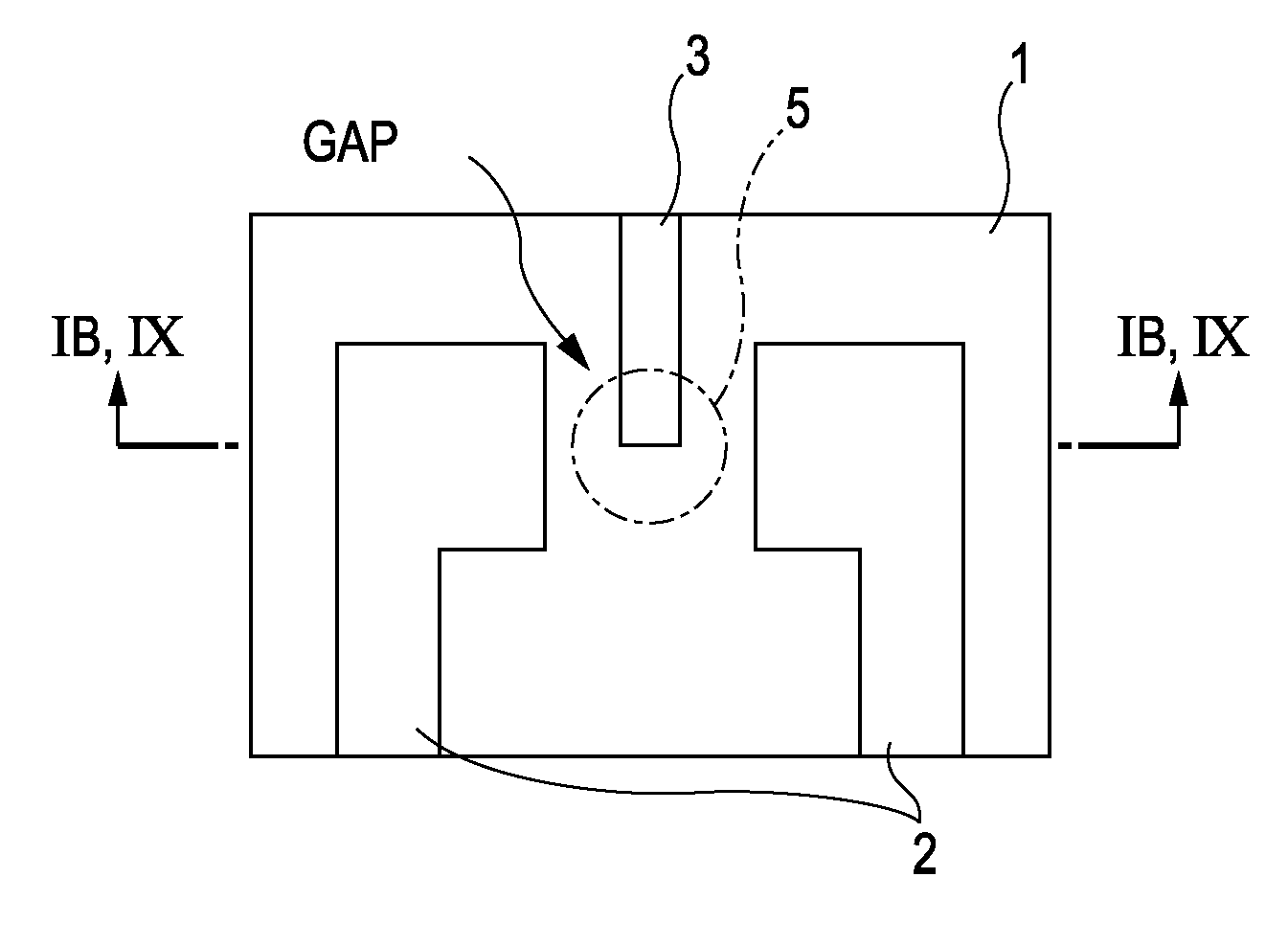
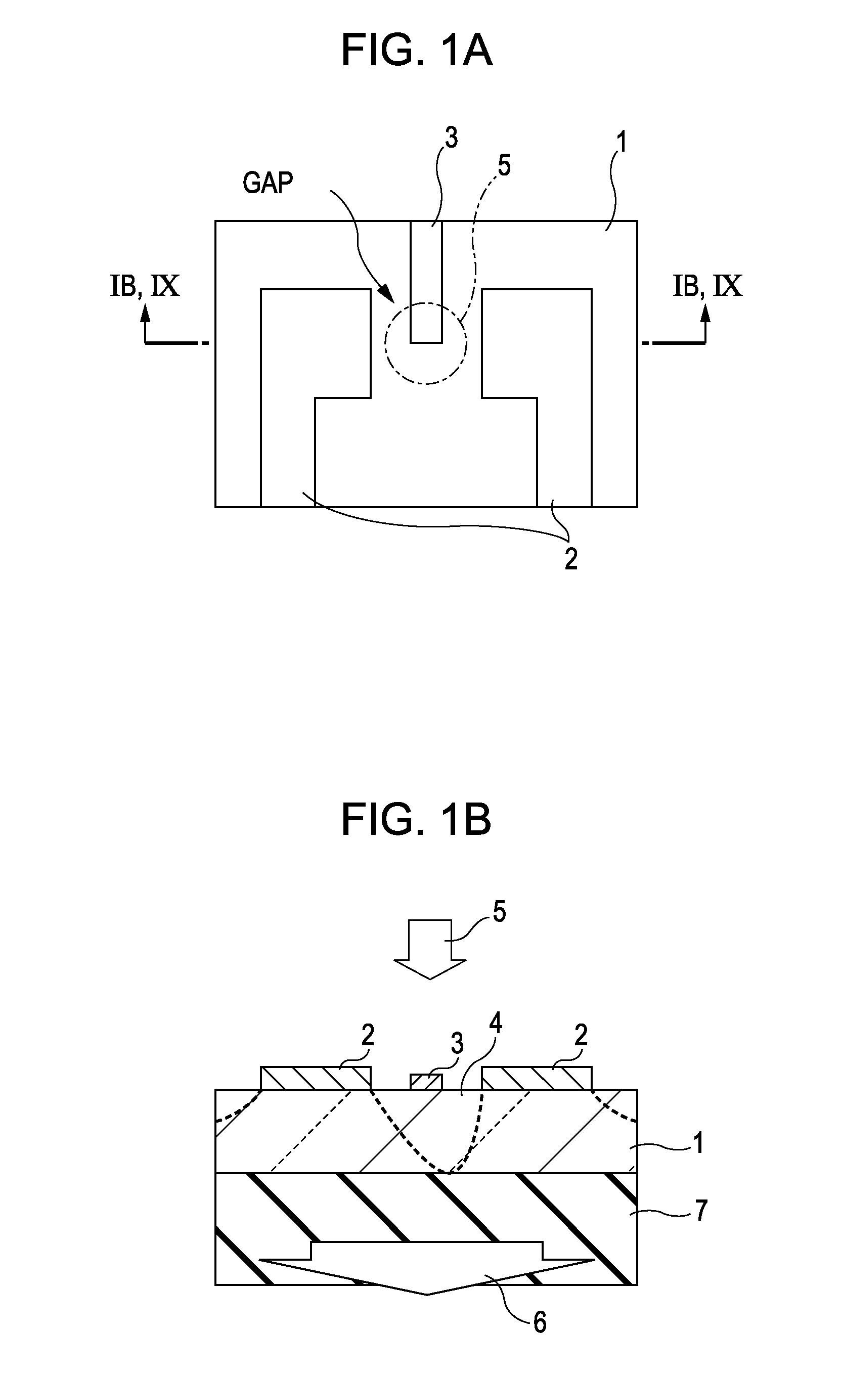
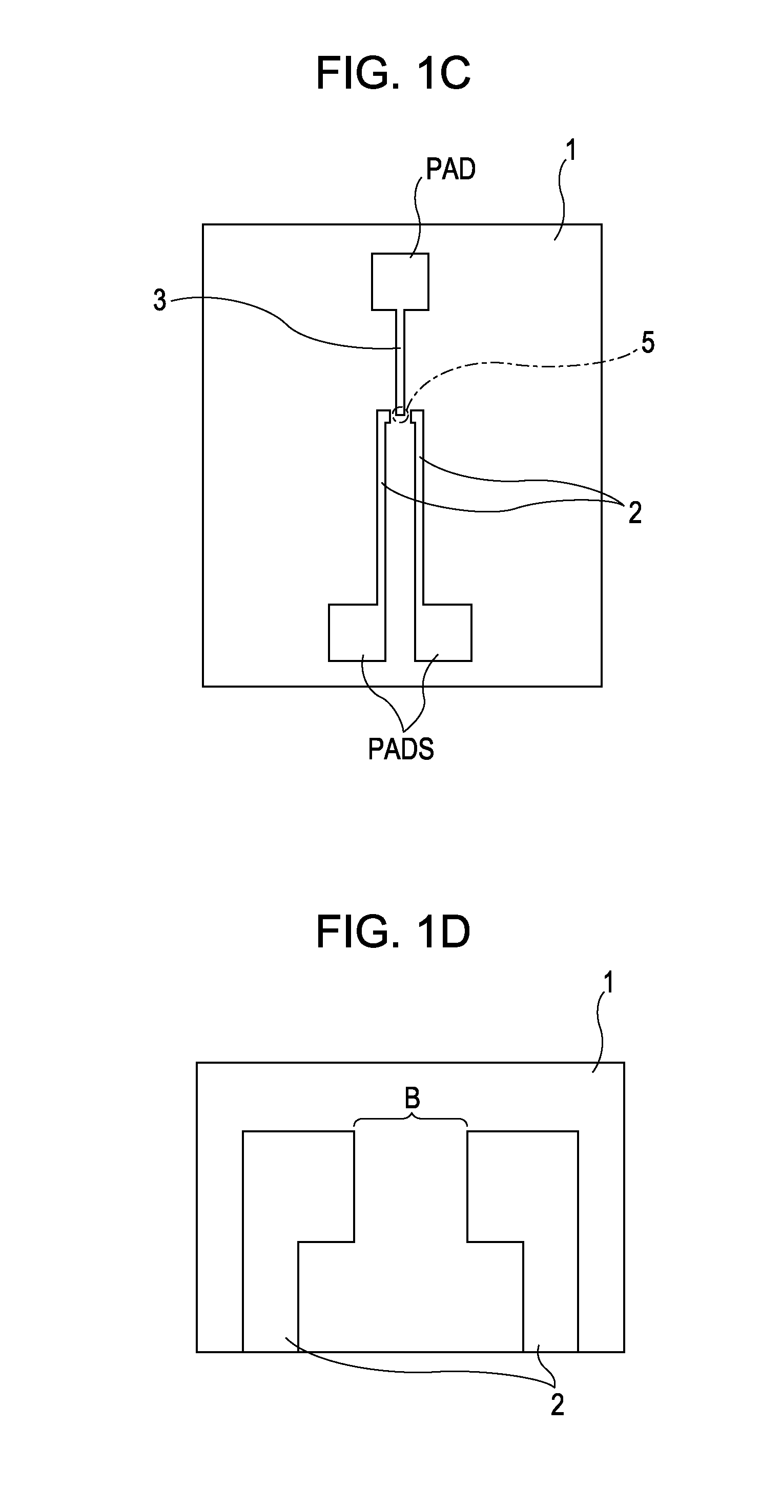
[0036]A photoconductive device according to a first embodiment of the invention is described. FIG. 1A is a top view of a general configuration of a photoconductive device according to the present embodiment, FIG. 1B is a sectional view taken along the line IB-IB of FIG. 1A, and FIG. 1C is a general view of the photoconductive device according to the present embodiment. FIG. 1A illustrates a magnified view of a portion of FIG. 1C where a terahertz wave 6 is generated by irradiation with excitation light 5. Referring to FIGS. 1A to 1C, the photoconductive device according to the present embodiment includes a substrate 7, a photoconductive layer 1, a pair of electrodes 2 constituted by first and second electrodes, and a third electrode 3. In the present embodiment, a group of electrodes is the pair of electrodes constituted by the first and second electrodes formed in such a manner as to be directly or indirectly in contact with the photoconductive layer 1. However, as long as an elect...

second embodiment

[0055]A second embodiment according to the photoconductive device of the present invention relates to a modification example of the above described photoconductive device. Descriptions of the common portions described above are omitted. FIG. 4A is a top view of a photoconductive device of the present embodiment and FIG. 4B is a sectional view taken along the line IVB-IVB of FIG. 4A. Referring to FIG. 4B, the difference from the photoconductive device of the first embodiment is that a third electrode 3 is arranged between a photoconductive layer 1 and a substrate 7. To manufacture the photoconductive device according to the present embodiment, it is necessary to arrange the third electrode 3 between the photoconductive layer 1 and the substrate 7. A transcription process can be used for this purpose. Here, for example, a buffer layer, an etch stop layer, and the photoconductive layer 1 are formed on a substrate made of an appropriate material, using a molecule beam epitaxial growth m...

third embodiment

[0058]A third embodiment according to the photoconductive device of the present invention relates to a modification example of the photoconductive devices described above. Descriptions of the common portions described above are omitted. FIG. 8A is a top view of a photoconductive device of the present embodiment and FIG. 8B is a sectional view taken along the line VIIIB-VIIIB of FIG. 8A. The difference from the above-described photoconductive devices is that a third electrode 3 is transparent to the wavelength of excitation light 5. An example of a material that can be used is ITO (indium tin oxide). By using a transparent electrode as the third electrode 3, the amount of the excitation light 5 input to a photoconductive layer 1 can be increased. Further, referring to FIGS. 8A and 8B, since the third electrode 3 does not block the excitation light 5, the third electrode 3 can be made larger than in the case illustrated in FIG. 1A. This makes it easy to control a depletion layer 4 in ...


PUM

PropertyMeasurementUnit
wavelength bandaaaaaaaaaa
temperatureaaaaaaaaaa

Abstract

A photoconductive device includes: a photoconductive layer configured to generate carriers upon irradiation with excitation light, a first electrode arranged on the photoconductive layer, a second electrode arranged on the photoconductive layer with a gap between the first and second electrodes, and a third electrode arranged in a region over which an electric field caused by voltages applied to the first and second electrodes or an electric field caused by irradiation with a terahertz wave extends. A depletion layer of the photoconductive layer is controllable by a voltage applied to the third electrode.

Description

BACKGROUND OF THE INVENTION[0001]1. Field of the Invention[0002]The present invention relates to a photoconductive device. The present invention also relates to a terahertz wave generation apparatus and a terahertz wave detection apparatus that each use the photoconductive device.[0003]2. Description of the Related Art[0004]Terahertz waves are electromagnetic waves having any components of frequency bands within a range from 0.03 THz to 30 THz. In the terahertz wave band, there exist many characteristic absorptions that depend on the structures and states of various materials including biological molecules. Utilizing such a characteristic, nondestructive inspection technologies for analyzing and identifying materials have been developed. Terahertz waves are also expected to be applied to safe imaging technologies replacing X-ray technology and high-speed communications technologies.[0005]One of the important factors for making these technologies practically usable is the advance in ...

Claims


Application Information

Patent Timeline
Patent Type & Authority Applications(United States)
IPC IPC(8): G03G15/00G01J1/02G01N21/35G01N21/3581H01L31/14H01S1/02
CPCG01N21/3581H01S1/02H01L31/09
Inventor KAJIKI, KOUSUKE
Owner CANON KK
Why Eureka
Try Eureka