

Preparation process for carbon film tin-sprayed printed circuit board
A technology of printed circuit board and preparation process, which is applied in the direction of printed circuit manufacturing, printed circuit, and secondary treatment of printed circuit, etc. Curing effect and other issues
- Summary
- Abstract
- Description
- Claims
- Application Information
AI Technical Summary
Problems solved by technology
Method used
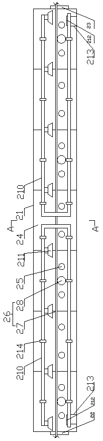
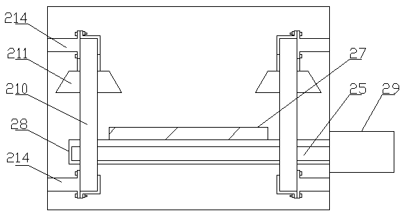
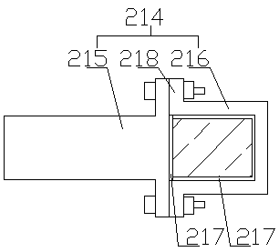
Image

Examples
Embodiment Construction
[0050] In order to make the technical solution of the present invention clearer, the present invention will be further described below in conjunction with the accompanying drawings. Any solution obtained by equivalent replacement and conventional reasoning of the technical features of the technical solution of the present invention falls within the protection scope of the present invention.
[0051] A carbon film spray tin printed circuit board preparation process, the steps are as follows:
[0052] (1) Pretreatment: Before solder mask and carbon film printing, use a mechanical scrubbing roughening cleaning machine to mechanically scrub and clean the copper plate substrate;
[0053] (2) Preparation of printing screen: use 220-mesh acrylic screen and coat with 30um thickness of sealing glue;
[0054] (3) Printing solder mask: Print ink on the printing screen; then print the printing screen with printing ink on the copper plate substrate; after printing the copper plate substrat...
PUM
 Abstract
Description
Claims
Application Information