Transceiving circuit for contactless communication

a technology of contactless communication and receiving circuit, which is applied in the direction of waveguide type devices, instruments, sensing record carriers, etc., can solve the problems of only achieving exact tuning, unstable voltage at the branching point of the receiving path rx from the first transmitting path tx, and detuning the antenna b>5/b>

Inactive Publication Date: 2010-12-23
NXP BV
View PDF1 Cites 29 Cited by
  • Summary
  • Abstract
  • Description
  • Claims
  • Application Information

AI Technical Summary

Benefits of technology

[0014]The characteristic features according to the invention provide the advantage that the voltage at the receiving path RX remains stable and essentially constant even in the event of varying loads at the antenna. Therefore, the dynamic range at the receiving path RX is greatly reduced so that amplifying and decoding circuits of the receiving section of the transmission module can be designed with less effort and higher performance. Further, it is achieved that the voltages at the receiving path RX always remain within a predefined range, even under negative influences of the environment, like external electromagnetic fields or external resonance circuits. Finally, the whole performance of the transceiving circuit is improved due to the fact that the voltage-level at the receiving path RX can be set higher compared with circuits according to prior art, because this voltage is not influenced by detuning of the antenna and due to the fact that higher voltages at the receiving path RX enable better demodulating of the received signals.
[0018]By switching an impedance matching network into the transmitting path(s) between DC decoupling capacitors and the antenna, a very high ratio of the power of the transmitted signals to the consumed electric power can be achieved.
[0019]In another embodiment of the invention a phase adjusting capacitor is switched into the receiving path, enabling to adjust the phase of signals between the transmission path and the receiving path, thereby achieving optimal demodulation.

Problems solved by technology

A disadvantage of these known transceiving circuits is, that the voltage at the branching point of the receiving path RX from the first transmitting path TX1 is not stable, but varies depending on the load onto the antenna 5.
However, exact tuning can only be achieved for one load state of the antenna 5 and hence varying loads inevitably result in detuning of the antenna 5.

Method used


Image

  • Transceiving circuit for contactless communication
  • Transceiving circuit for contactless communication
  • Transceiving circuit for contactless communication

Examples


Embodiment Construction

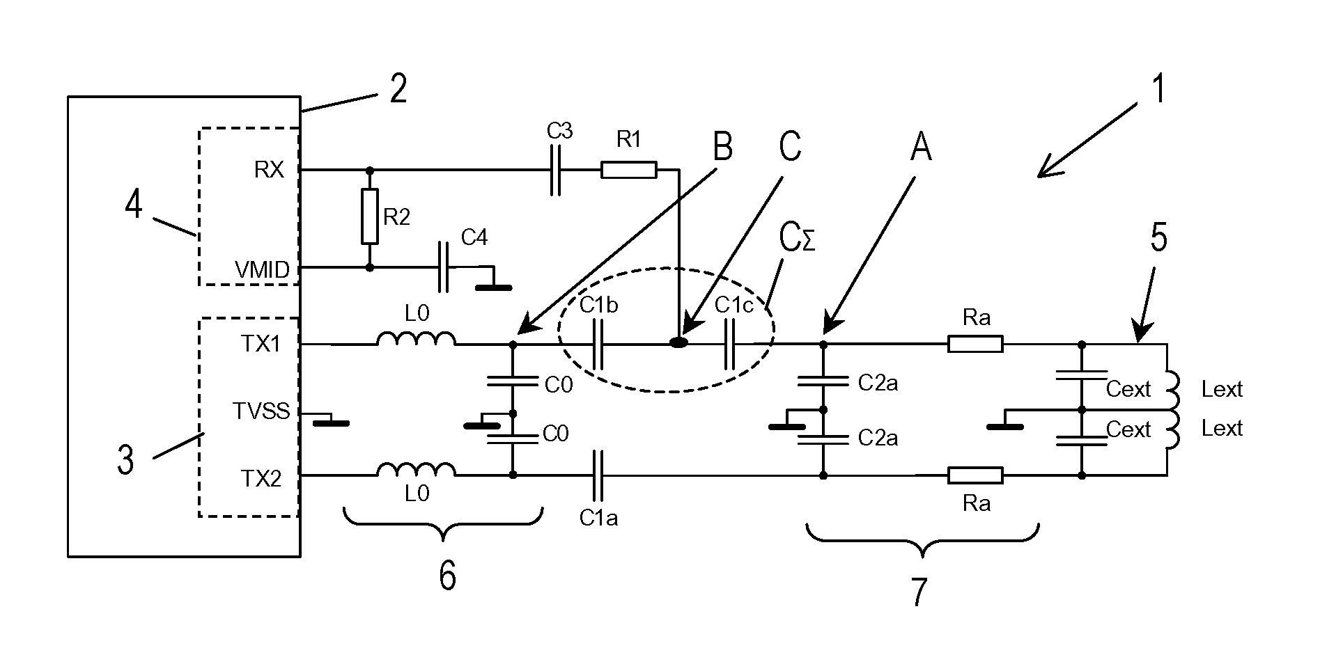
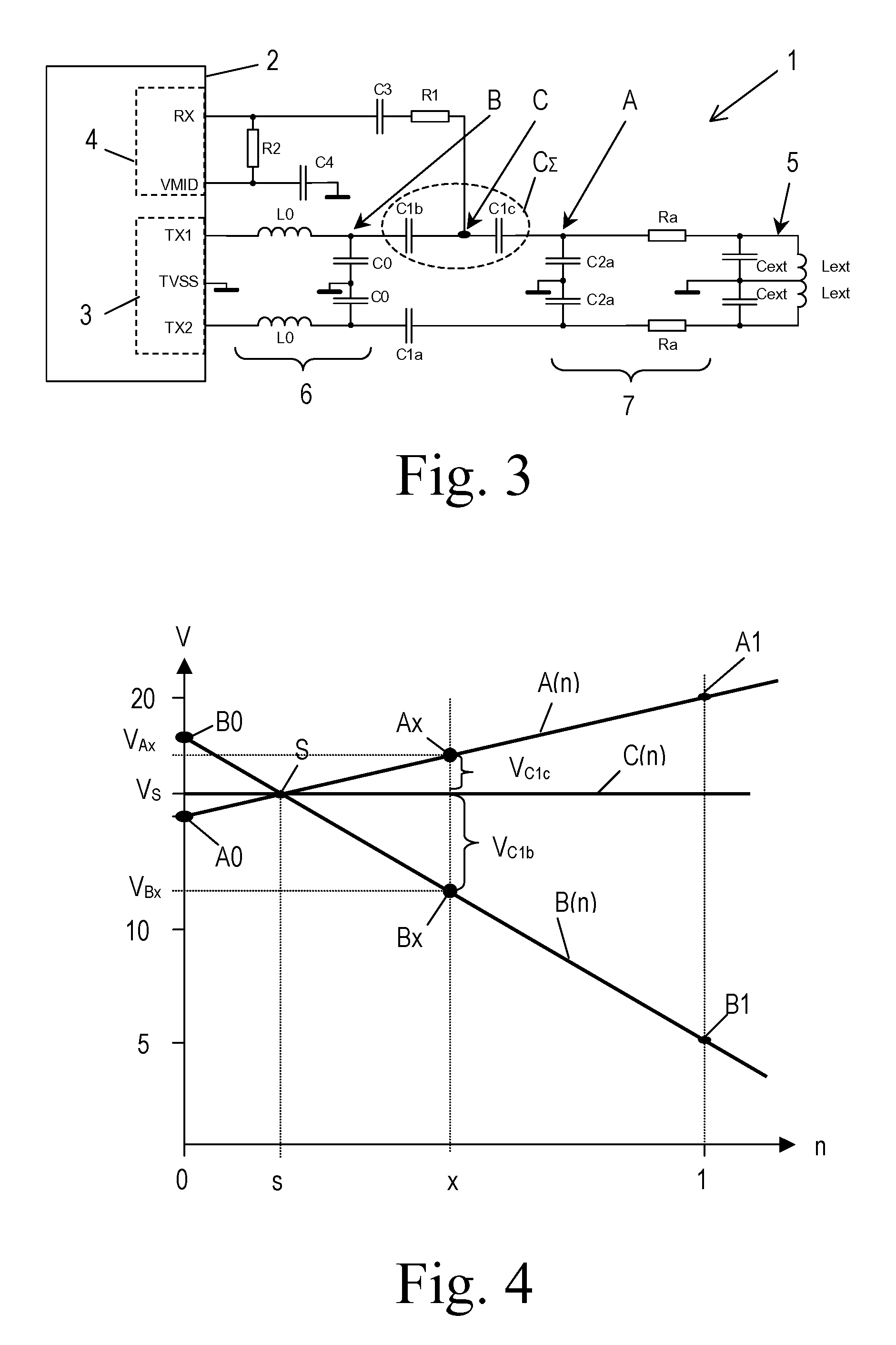
[0031]FIG. 3 shows a circuit diagram of a transceiving circuit 1 according to the present invention. This transceiving circuit comprises an integrated RFID transmission module 2, e.g. a Reader IC or a near field communication transmission module. The transmission module 2 comprises transmitter means 3 and receiver means 4.

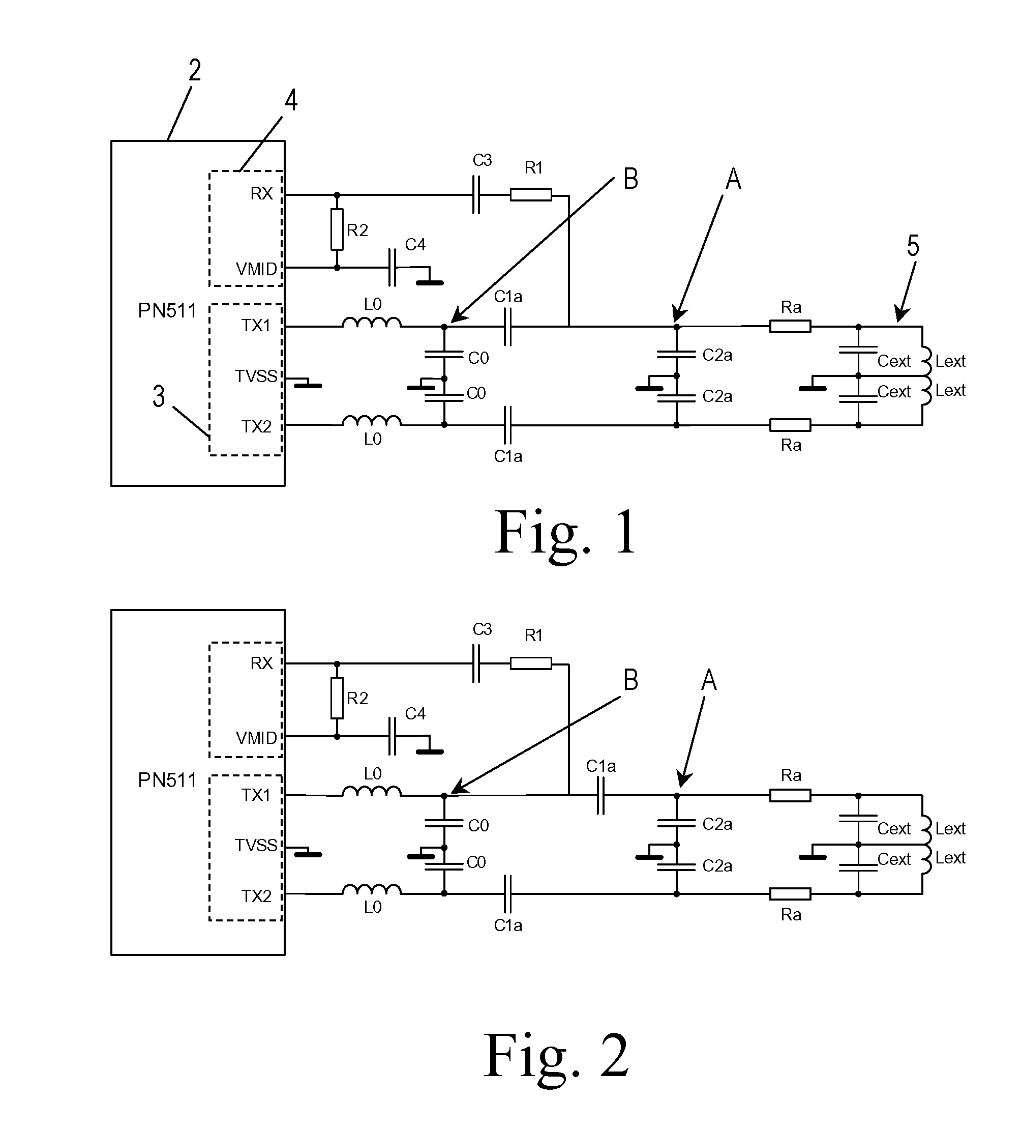
[0032]For a better understanding of the function of the RFID transmission module 2, a block diagram of the near field communication (NFC) transmission module type no. PN511 is shown in FIG. 7. The NFC transmission module 2 comprises analog circuitry which can be roughly divided into transmitter means 3 and receiver means 4. Although not shown, the analog circuitry comprises output drivers, an integrated demodulator, a bit decoder, a mode detector and an RF-level detector. A contactless UART communicates with the analog circuitry via a bus. The contactless UART comprises data processing means, CRC / Parity generation and checking means, frame generation and checking m...


PUM


Abstract

A transceiving circuit (1) for contactless communication comprises transmitter means (3) to generate an electromagnetic carrier signal, to modulate the carrier signal according to transmitting data and to drive an antenna (5) with the modulated carrier signal, and receiver means (4) to sense response signals being received at the antenna (5) and to demodulate the response signals. The transmitter means (3) are connected to the antenna (5) by at least a first transmitting path (TX1), wherein a first DC decoupling capacitor (C1b) is switched into the first transmitting path (TX1). A receiving path (RX) branches off from the first transmitting path (TX1) to the receiver means (4). A second DC decoupling capacitor (C1c) is switched into the first transmitting path (TX1) in series to the first DC decoupling capacitor (C1b). The receiving path (RX) branches off from the first transmitting path (TX1) at a branching point (C) between the first and second DC decoupling capacitors (C1b, C1c).

Description

FIELD OF THE INVENTION[0001]The invention relates to a transceiving circuit for contactless communication comprising:[0002]transmitter means being adapted to generate an electromagnetic carrier signal, to modulate the carrier signal according to transmitting data and to drive an antenna with the modulated carrier signal, receiver means being adapted to sense response signals being received at the antenna and to demodulate the response signals, wherein the transmitter means are connected to the antenna by means of at least a first transmitting path, wherein a first DC decoupling capacitor is switched into the first transmitting path, wherein a receiving path branches off from the first transmitting path to the receiver means.[0003]The invention further relates to an NFC device or an RFID reader / writer device.BACKGROUND OF INVENTION[0004]FIGS. 1 and 2 show known implementations of transceiving circuits for contactless communication. These transceiving circuits employ an integrated nea...

Claims


Application Information

Patent Timeline
Patent Type & Authority Applications(United States)
IPC IPC(8): H03H7/48
CPCG06K7/0008G06K7/10316G06K7/10237
Inventor MERLIN, ERICH
Owner NXP BV
Why Eureka
Try Eureka