Passive-matrix chiplet drivers for displays

a technology of matrix chiplet and display device, which is applied in the direction of semiconductor devices, instruments, electrical devices, etc., can solve the problems of affecting the inability the inability to accurately measure the current required to drive an entire row (or column) of the display, etc., to achieve the reduction of the size and number of chiplets, the effect of improving the uniformity and luminance of the display devi

Active Publication Date: 2010-12-30
GLOBAL OLED TECH
View PDF16 Cites 17 Cited by
  • Summary
  • Abstract
  • Description
  • Claims
  • Application Information

AI Technical Summary

Benefits of technology

[0016]The present invention has the advantage that chiplet pixel drivers provide improved uniformity and luminance in a display device. By providing a display device with chiplet drivers having row and column electrode connections to row and column electrodes forming pixels, the number of connection pads and the size and number of chiplets are reduced. A plurality of pixel groups provides reduced flicker and power requirements. Another advantage of the present invention is that, by employing chiplets that drive both row and column electrodes, chiplet utilization is improved and, when laid out with chiplet portions associated with rows or columns of pixel groups, wiring difficulties are reduced and aperture ratio increased. Furthermore, the distribution of heat from chiplets is improved and the number of different chiplets can be reduced.

Problems solved by technology

However, a passive-matrix drive device is limited in the number of rows (or columns) that can be included in the device since the sequential nature of the row (or column) driving creates flicker.
If too many rows are included, the flicker can become perceptible.
Moreover, the currents necessary to drive an entire row (or column) in a display can be problematic and the power required for the non-imaging pre-charge and discharge steps of PM driving become dominant as the area of the PM display grows.
These two problems limit the physical size of a passive-matrix display.
Thin-film transistors (TFTs) made from amorphous or polycrystalline silicon are relatively large and have lower performance compared to conventional transistors made in crystalline silicon wafers.
Moreover, such thin-film devices typically exhibit local or large-area non-uniformity across the glass substrate that results in non-uniformity in the electrical performance and visual appearance of display employing such materials.
Since a conventional passive-matrix display design is limited in size and number of light-emitting elements, and an active-matrix design using TFTs has lower electrical performance, there is a need for improved control for display devices employing LEDs that overcomes these problems.

Method used


Image

  • Passive-matrix chiplet drivers for displays
  • Passive-matrix chiplet drivers for displays
  • Passive-matrix chiplet drivers for displays

Examples


Embodiment Construction

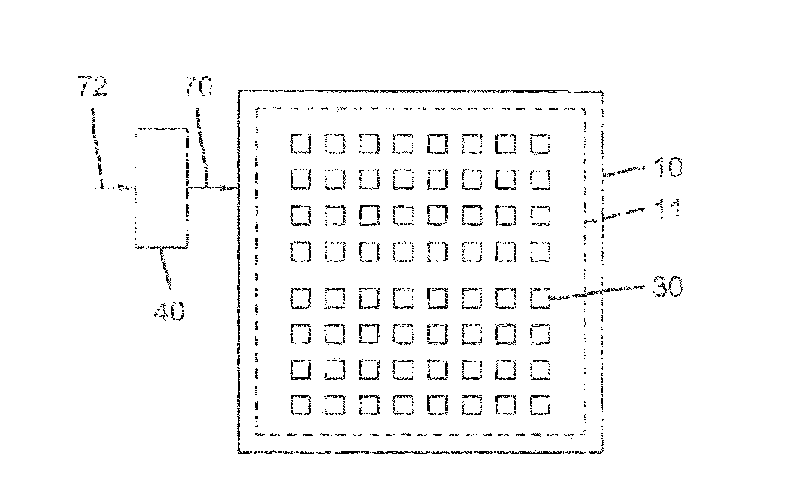
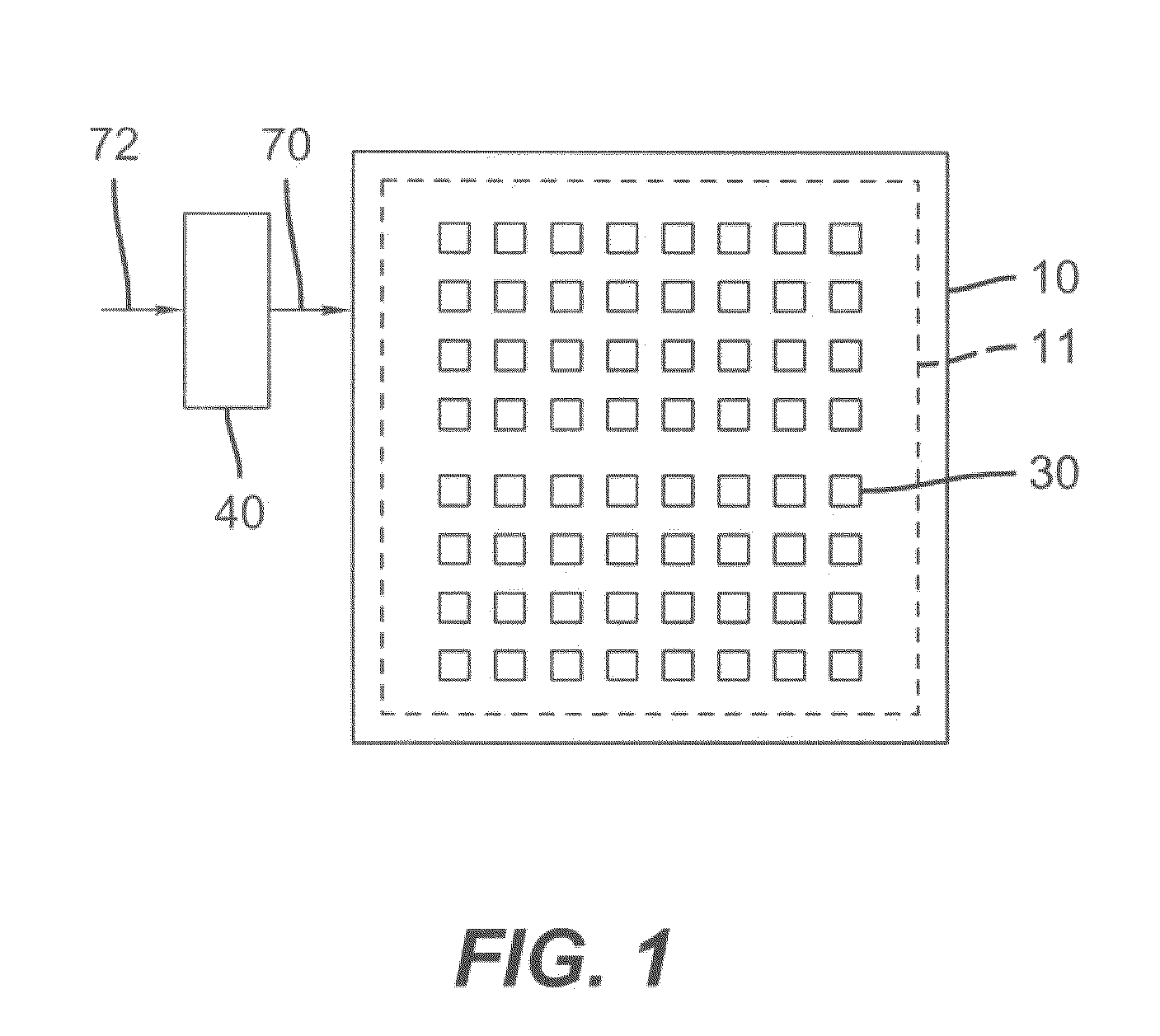
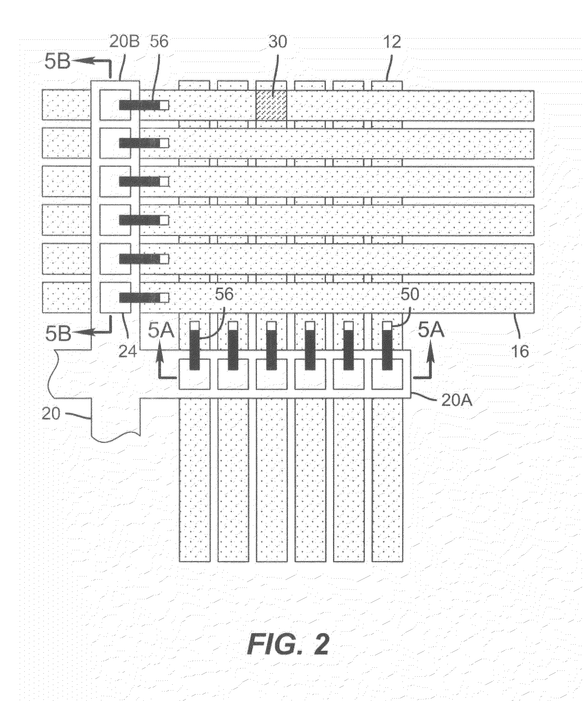
[0031]Referring to FIG. 1, in one embodiment of a display device according to the present invention, a substrate 10 has a display area 11 including a two-dimensional array of pixels 30 located in the display area 11. A controller 40 is connected to and can control the display device through control signals 70 in response to image signals 72. As shown in FIGS. 2 and 3, a plurality of independent column electrodes 12 extend in a column direction in a first layer, a plurality of row electrodes 16 extends in a row direction different from the column direction in a second layer. A layer of light-emitting materials is located between the first and second layers; the pixels 30 in the two-dimensional array of pixels 30 are formed where the column electrodes 12 and row electrodes 16 overlap.

[0032]As used herein, a plurality of independent column electrodes 12 extending in a column direction means that the display device must have at least two electrically independent column electrodes 12 ext...


PUM


Abstract

A passive-matrix display device having a plurality of chiplets, each chiplet associated with one or more independent column electrodes located in the display area, each chiplet electrically connected to and driving a separate subset of the independent column electrodes and electrically connected to and driving a subset of the row electrodes to cause the light-emitting material in each pixel to emit light, wherein each chiplet includes a serial luminance shift register for shifting pixel luminance values corresponding to each independent column electrode from one chiplet to another and a column driver for driving each of the independent column electrodes to which it is connected with the corresponding pixel luminance values; and wherein each chiplet further includes a row driver for driving each corresponding row electrode to which it is connected and a row control shift register for controlling the row drivers.

Description

CROSS REFERENCE TO RELATED APPLICATIONS[0001]Reference is made to commonly assigned U.S. Patent Application Ser. No. 12 / 372,906, filed Feb. 18, 2009, entitled Display Device With Chiplet Drivers, by Ronald S. Cok, et al; Ser. No. 12 / 371,666, filed Feb. 16, 2009, entitled Chiplet Display Device With Serial Control, by Ronald S. Cok; Ser. No. 12 / 424,060, filed Apr. 15, 2009, entitled Display Device With Polygonal Chiplets, by Ronald S. Cok, and Ser. No. 12 / 431,925, filed Apr. 29, 2009, entitled Chiplet Display With Oriented Chiplets And Busses, by Ronald S. Cok, the disclosures of which are incorporated herein.FIELD OF THE INVENTION[0002]The present invention relates to passive-matrix display devices having particular chiplet configurations for facilitating improved operation.BACKGROUND OF THE INVENTION[0003]Flat-panel display devices are widely used in conjunction with computing devices, in portable devices, and for entertainment devices such as televisions. Such displays typically e...

Claims


Application Information

Patent Timeline
Patent Type & Authority Applications(United States)
IPC IPC(8): G09G3/30
CPCG09G3/2085G09G3/3216G09G3/3266G09G3/3275H01L27/3255G09G2310/0221G09G2310/0278G09G2310/0286G09G2320/0247G09G2300/0465H10K59/129G09G3/32H10K59/00
Inventor COK, RONALD S.
Owner GLOBAL OLED TECH
Why Eureka
Try Eureka