Structured material substrates for flexible, stretchable electronics

a technology of structural materials and electronics, applied in the direction of dielectric characteristics, semiconductor/solid-state device details, transportation and packaging, etc., can solve the problems of not fully achieving the desired flexibility and stretchability, introducing additional manufacturing/assembly challenges and costs, and neither approach has yet provided a large-scale commercial flexible/stretchable electronic technology

Active Publication Date: 2010-12-30
INFINITE CORRIDOR TECH
View PDF33 Cites 153 Cited by
  • Summary
  • Abstract
  • Description
  • Claims
  • Application Information

AI Technical Summary

Benefits of technology

[0015]According to another aspect of the invention, there is provided a method of forming a flexible and stretchable patterned substrate. The method includes providing a strain-permitting material. Also, the method includes forming a patterned

Problems solved by technology

These solutions have only partially achieved the desired flexibility and stretchability, while introducing additional manufacturing/assembly challenges and costs.
Due to fundamental limitations with the developments which have been made thus far, neither approach has yet to provide a large-scale commercial flexible/stretchable electronic technology.
Problems related to the attachment of commercial electronic components to the stretching substrate without transmission of forces that will tend to either fracture or detach the components have not been resolved in a manner compatible with current industrial electronic manufacturing processes.
Furthermore, a fundamental limitation of this approach is that current polymeric conductive materials have excessive impedance, severely limiting the applications that can employ these materials.
Stretchable devices using unsupported metal interconnects suffer from two primary problems.
First, these approaches introduce a number of challenging intermediate fabrication steps, completely incompatible with conventional industrial electronic manufacturing processes.
Second, these devices are prone to failure when deformed, as either the unsupported leads or the connection of the leads to the substrate carrying the electronic components tend to fail under the forces necessary to stretch the interconnects.
This approach only

Method used


Image

  • Structured material substrates for flexible, stretchable electronics
  • Structured material substrates for flexible, stretchable electronics
  • Structured material substrates for flexible, stretchable electronics

Examples


Embodiment Construction

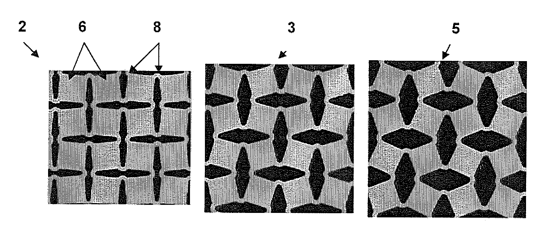
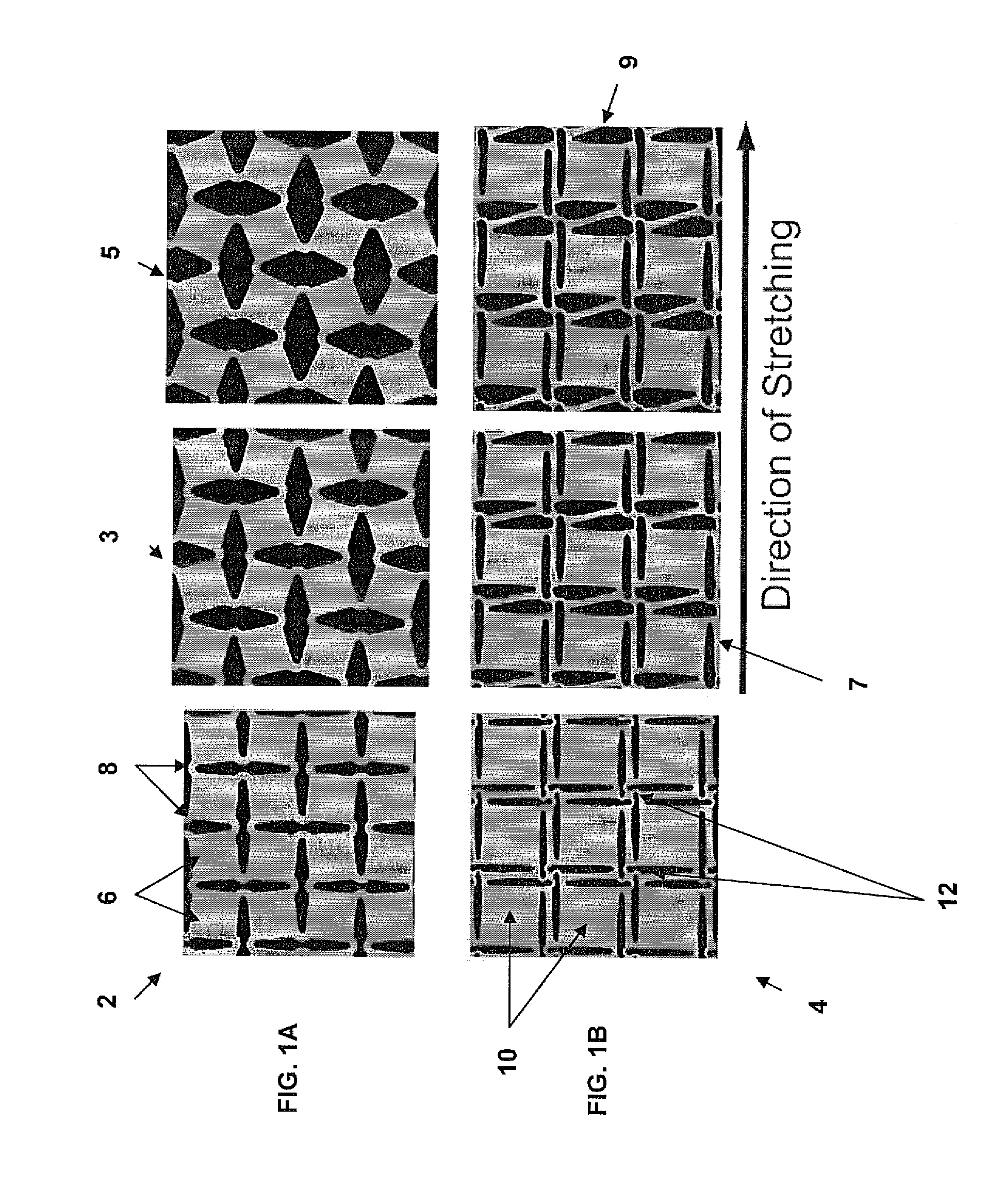
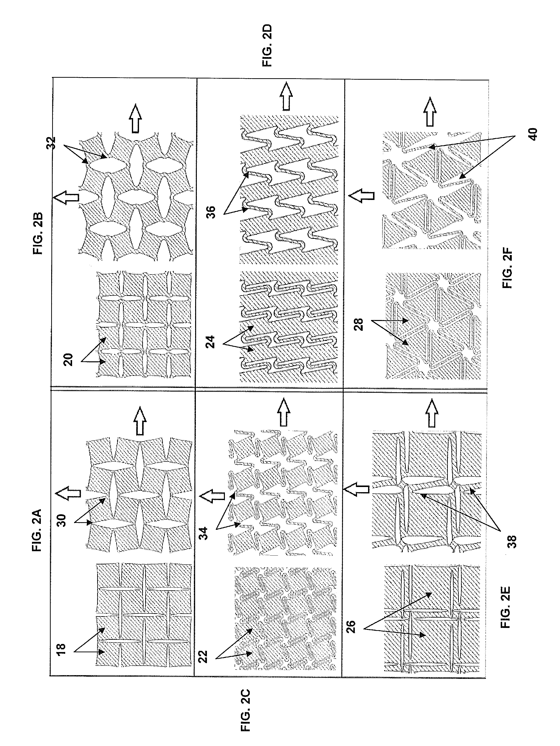
[0022]The invention provides a design for flexible stretchable and conformable substrates for integrated devices and method to manufacture stretchable, flexible and conformable integrated devices, including electronics, photovoltaics, antennas, and other integrated devices. A complete integrated device consists of a base substrate, with a system of conductive interconnects or “traces”, housing the necessary components (electronic components for an electronic device, photovoltaic cells for a photovoltaic device, etc.). The base substrate with the conductive interconnects will hereafter be referred to as a printed circuit board or PCB. The electronic (or photovoltaic, or sensor, etc.) components will hereafter be referred to as simply components or chips.

[0023]The integrated device includes a flexible structured material substrate (SMS) having a patterned conformation that allows the substrate to experience local strains lower than the macroscopic strain imposed on the integrated devi...


PUM

PropertyMeasurementUnit
Flexibilityaaaaaaaaaa
Strain pointaaaaaaaaaa
Stretchabilityaaaaaaaaaa

Abstract

A flexible and stretchable patterned substrate is provided having a strain-permitting material comprising a patterned conformation that allows the flexible patterned substrate to experience local strain or local strain domains lower than the macroscopic strain of the flexible and stretchable patterned substrate.

Description

PRIORITY INFORMATION[0001]This application claims priority from provisional applications Ser. No. 61 / 221,542 filed Jun. 29, 2009, Ser. No. 61 / 265,256 filed Nov. 30, 2009, and Ser. No. 61 / 320,747 filed Apr. 4, 2010, all of which are incorporated herein by reference in their entireties.BACKGROUND OF THE INVENTION[0002]The invention relates to the field of stretchable, flexible and conformable integrated devices, including electronics, photovoltaics, antennas, and other integrated devices. In particular the invention relates to substrate designs that exhibit regions with low strain when subjected to larger macroscopic strain.[0003]Current, large-scale commercial technology for integrated electronic devices is primarily based on rigid (stiff) printed circuit boards. The rigid boards serve as the support for the electronic components and conductive interconnects (traces), and also limit the magnitudes of strain and stress that are transmitted to the components and traces. It is necessary...

Claims


Application Information

Patent Timeline
IPC IPC(8): B32B3/00B29C71/00
CPCB29C59/02Y10T428/24479B29C2791/009B29C2793/00H01L23/4985H01L2924/3011H05K1/0283H05K2201/0133H05K2201/09063B32B3/266H01L2924/0002B29C59/16Y10T428/24314H01L2924/00H05K2201/046
Inventor BOYCE, MARY C.SOCRATE, SIMONABOYCE, CHRISTOPHER M.GREVISKES, BRIAN P.
Owner INFINITE CORRIDOR TECH
Why Eureka
Try Eureka