Display device

a display device and circuit chip technology, applied in static indicating devices, identification means, instruments, etc., can solve the problems of high connection resistance between bumps and wiring line terminals, unstable, unstable, etc., to reduce the electric resistance, reduce power loss, and reduce the effect of terminal portions

Active Publication Date: 2005-03-10
PANASONIC LIQUID CRYSTAL DISPLAY CO LTD +1
View PDF3 Cites 47 Cited by
  • Summary
  • Abstract
  • Description
  • Claims
  • Application Information

AI Technical Summary

Benefits of technology

[0029] The first advantageous effect lies in the reduction of the power loss and the delay or the strain of signals at a bonding portion of the first bump of the drive circuit element and the terminal portion formed on the main surface of the insulation substrate using the anisotropic conductive film. The advantageous effect can be obtained due to the reduction of the electric resistance between the first bump and the terminal portion via the bonding portion. As the bonding portion between the first bump and the terminal portion becomes spaced further away from one side of the mounting surface of the drive circuit element, the bonding portion is more surely isolated from the atmosphere in which the display device is used due to the main surface of the insulation substrate, the mounting surface of the drive circuit element which faces the insulation substrate and the anisotropic conductive film, and, hence, the electric resistance between the first bump and the terminal portion can be maintained at a low level in a stable manner for a long period.
[0030] Another advantage lies in the fact that, in a step in which, in a state where the mounting surface of the drive circuit element is arranged to face the anisotropic conductive film which is formed on the peripheral portion of the main surface of the insulation substrate (including the mounting portion of the main surface), the thermo-compression bonding head is brought into contact with an upper surface (side opposite to the mounting surface) of the drive circuit element so as to bond the bumps (respective bumps including the above-mentioned first bumps) formed on the mounting surface of the drive circuit element and terminal portions formed on the peripheral portion of the main surface of the insulation substrate, no residual stress is applied to the anisotropic conductive film which is sandwiched between the first bumps and the terminal portions so as to bond them and, at the same time, the reliability of bonding between first bumps and the terminal portions is not damaged. Since the first bumps are positioned inside the mounting surface of the drive circuit element (being remote from one side of the mounting surface), in this bonding step, the influence that the inclination of the thermo compression bonding head, which is brought into contact with the upper surface of the drive circuit element, with respect to the upper surface affects the bonding (thermo compression bonding) of the first bumps and the terminal portions can be reduced.
[0031] In the display device in which the structure 2 is introduced, the second bumps and the first bumps which are arranged close to the second bumps assume the same potential and, hence, the parasitic capacitance which is generated along the wiring lines which are connected to the first bumps can be reduced. Accordingly, the distortion of waveforms which are generated with signals which are transmitted through the wiring lines also can be suppressed. Even when the second bumps are brought into contact with the wiring lines which are connected with the first bumps that are arranged close to the second bumps, the second bumps and the first bumps may become conductive to each other or assume the same potential in the drive circuit element. On the other hand, when the second bumps face the wiring lines which are connected with the first bumps arranged close to the second bumps by way of an insulation film, no potential difference is substantially generated between an upper surface and a lower surface of the insulation film, and, hence, there is no possibility that the conductive film (particularly th

Problems solved by technology

In mounting a drive circuit chip using the COG method, a phenomenon, in which the connection resistance between the bumps formed at four corners of the drive circuit chip IC and the input/output wiring line terminals formed on the insulation substrate is increased or the resistance value becomes unstable, is liable to be easily generated.
Accordingly, there exists a possibility that the connection resistance between the bumps and the wiring line terminal portions which interpose the anisotropic conductive film therebetween in the vicinities of the two corners of the

Method used


Image

  • Display device
  • Display device
  • Display device

Examples


embodiment 1

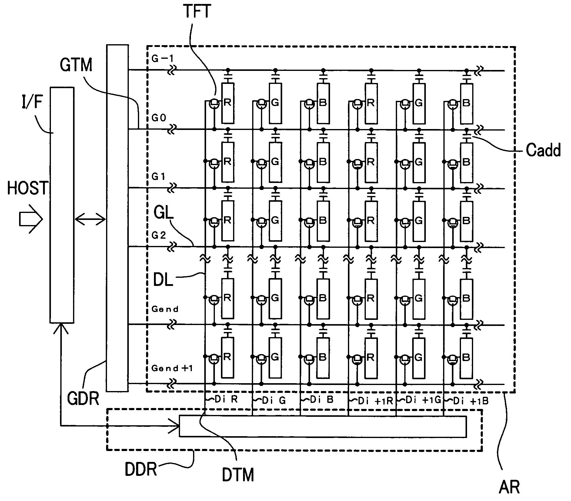
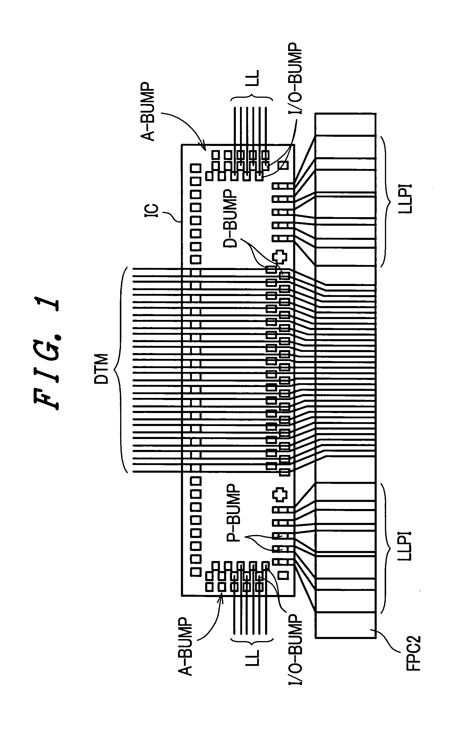
[0051]FIG. 1 is a plan view showing an example of the structure around a drive circuit chip (an integrated circuit element referred to as a drive circuit element) according to this embodiment, which drive circuit chip is mounted on an end periphery of a main surface of one substrate of a liquid crystal display panel, wherein the drawing shows a state in which a flexible printed circuit board is mounted on the wiring line for inputting drive circuit power. The drive circuit chip IC of this embodiment is used for driving drain lines which supply display data to drains of thin film transistors which constitute pixels. The drive circuit chip IC includes a plurality of first input / output bumps I / O-BUMP and a plurality of second input / output bumps A-BUMP on both short-sides of a mounting surface (a surface facing the insulation substrate, also referred to as a circuit surface or a front-side surface). Further, on one of the long sides which are positioned at an outer periphery of the insu...

embodiment 2

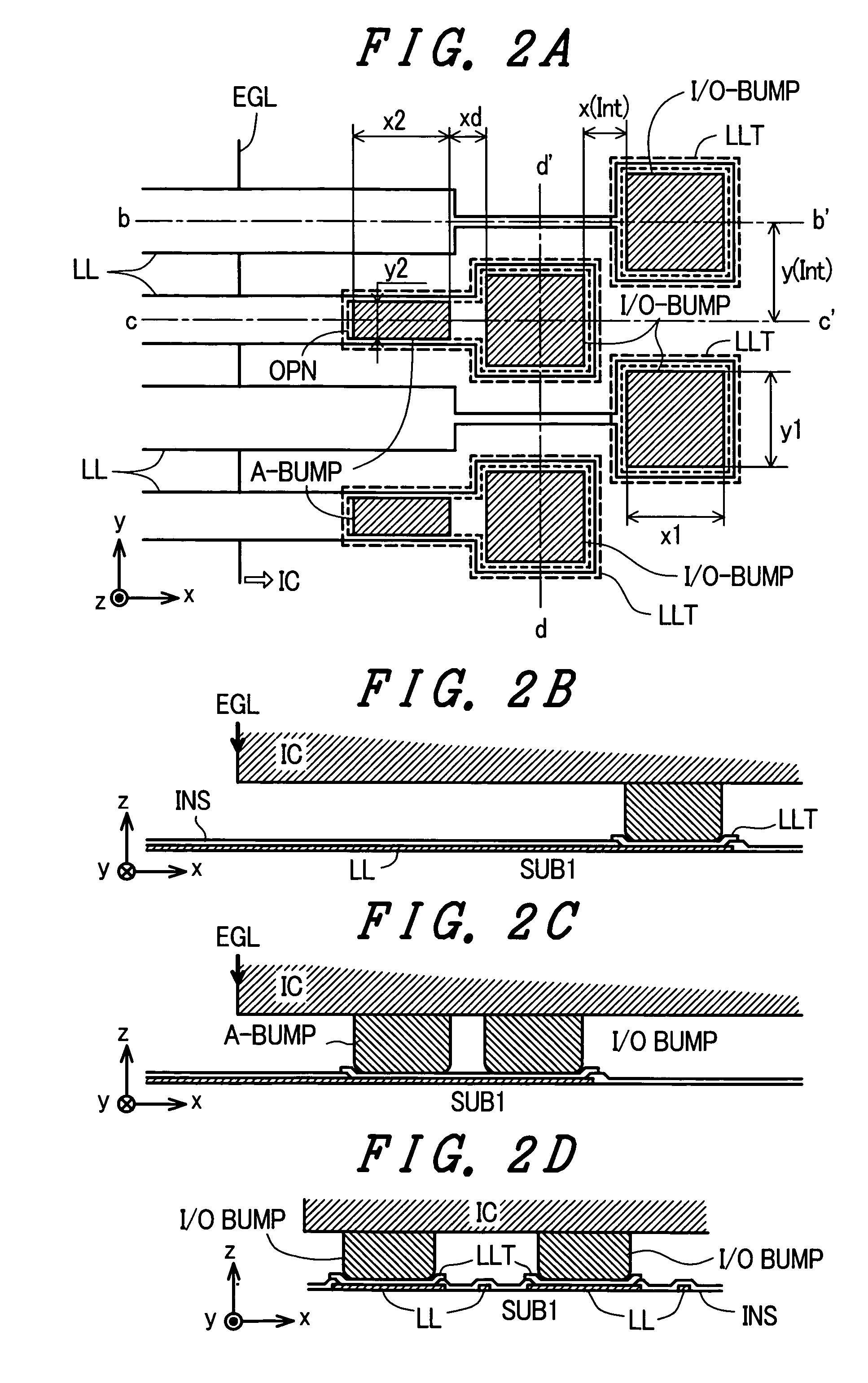
[0068]FIG. 3 is a partially enlarged plan view showing the constitution of the input / output wiring lines LL at the left short side and the first input / output bump and the second input / output bump provided to the drive circuit chip IC. The line EGL shown in FIG. 3 indicates a chip end of the drive circuit chip IC in the same manner as FIG. 2A. In this embodiment, out of the LCD terminals LLT which are alternately arranged, the LCD terminals LLT of the input / output wiring lines LL close to the chip end EGL side of the drive circuit chip IC are enlarged toward the chip end EGL side of the drive circuit chip IC. The width of the LCD terminal LLT in the direction parallel to the chip end EGL is set to a size (a size to cover, the term used in this meaning hereinafter) which includes first input / output bumps I / O-BUMP, wherein the length in the direction perpendicular to the chip end EGL is a size which includes the first input / output bumps I / O-BUMP and the second input / output bump A-BUMP....

embodiment 3

[0072]FIG. 4 is a partially enlarged plan view showing the constitution of the input / output wiring lines LL at the left short side in FIG. 1 and the first input / output bump and the second input / output bump provided to the drive circuit chip IC. This embodiment is characterized in that the second input / output bump A′-BUMP in the embodiment 2 has the same shape as the first input / output bump A-BUMP. In this embodiment, out of the LCD terminals LLT which are alternately arranged, the LCD terminals LLT of the input / output wiring lines LL close to the chip end EGL side of the drive circuit chip IC are enlarged toward the chip end EGL side of the drive circuit chip IC and are connected such that the LCD terminal LLT includes the first input / output bump I / O-BUMP and the second input / output bump A′-BUMP. The other features of this embodiment are substantially equal to the corresponding constitutions of the embodiment 2. Also, according to this embodiment, the previously-mentioned residual s...


PUM


Abstract

To prevent the peeling-off of a drive circuit chip from an insulation substrate of a display device attributed to a residual stress between terminals formed on the insulation substrate and bumps formed on a mounting surface of a drive circuit chip, as well as to stabilize the connection resistance therebetween, the present invention provides an auxiliary bump for one of the bumps on the mounting surface of the drive circuit chip at an end edge side thereof with respect to the one of the bumps and arranges the auxiliary bump electrically in contact with one of the terminals formed on the insulation substrate of the display device with which the one of the bumps also is in electrical contact. Since the one of the bumps is spaced from the end edge side of the mounting surface of the drive circuit chip by the auxiliary bump, electrical contact thereof with the one of the terminals cannot be affected by the atmospheres in which the display device is used, and distortion of a signal waveform caused thereat can be suppressed also.

Description

[0001] The present application claims priority from Japanese application JP 2003-294089 filed on Aug. 18, 2003, the content of which is hereby incorporated by reference into this application. BACKGROUND OF THE INVENTION [0002] The present invention relates to the drive circuit chip mounting structure for use in a display device, and, more particularly, to a so-called flip-chip mounting type (or a chip-on-glass type) display device in which drive circuit chips are directly mounted on the periphery of a substrate which constitutes a display panel of the display device. [0003] An active matrix type display device, which includes active elements, such as thin film transistors, for respective pixels and performs a switching driving of these active elements, is a known type of panel type display device, and it is exemplified by a liquid crystal display device or an organic EL display device. The present invention is characterized by the mounting structure of the drive circuit chips on a d...

Claims


Application Information

Patent Timeline
IPC IPC(8): G02F1/1345G02F1/13G02F1/133G09F9/00G09G3/36G09G5/00H01L21/60H01L23/498H01L51/50H05B33/06H05B33/14
CPCG02F1/13452H01L23/49816H01L2924/00011H01L2224/293H01L2224/2929H01L2224/17515H01L2224/83851H01L23/49838H01L24/83H01L2224/13144H01L2224/16H01L2224/29075H01L2924/00014H01L2924/14H01L2924/00G02F1/133G02F1/1345
Inventor TAKENAKA, YUUICHINAKAYAMA, TAKANORI
Owner PANASONIC LIQUID CRYSTAL DISPLAY CO LTD
Why Eureka
Try Eureka