

Nitride semiconductor light-emitting device and method for fabrication thereof
Active Publication Date: 2005-02-03
SHARP FUKUYAMA LASER CO LTD
View PDF19 Cites 44 Cited by
- Summary
- Abstract
- Description
- Claims
- Application Information
AI Technical Summary
Benefits of technology
[0011] In view of the conventionally encountered problems mentioned above, it is an object of the present invention to provide a nitride semiconductor light-emitting device, such as a nitride semiconductor laser device, that uses a substrate with low defect density, that c
Problems solved by technology
Moreover, even if cracks develop, their development is limited
Method used
View moreImage
Smart ImageViewing Examples

Examples
 PUM
 Abstract
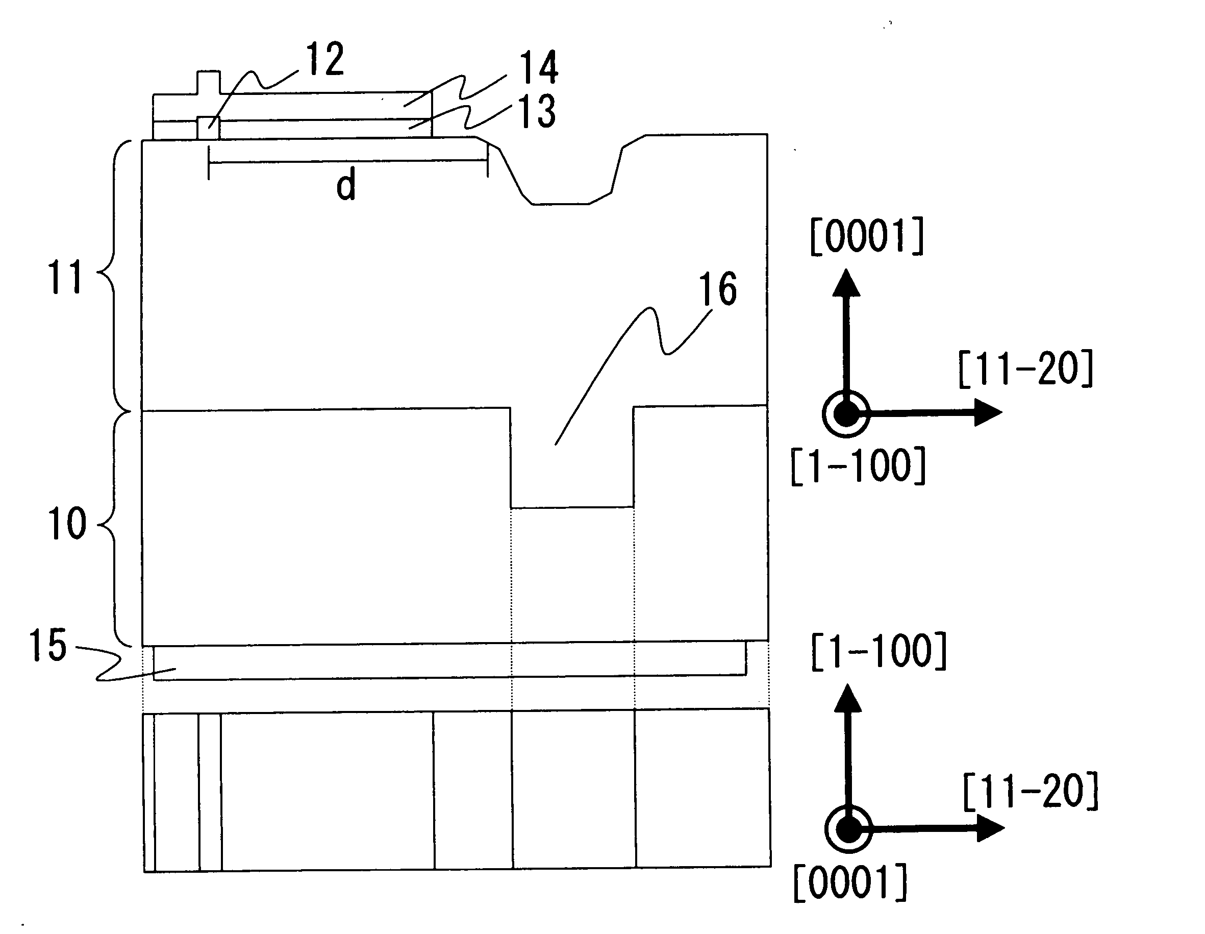
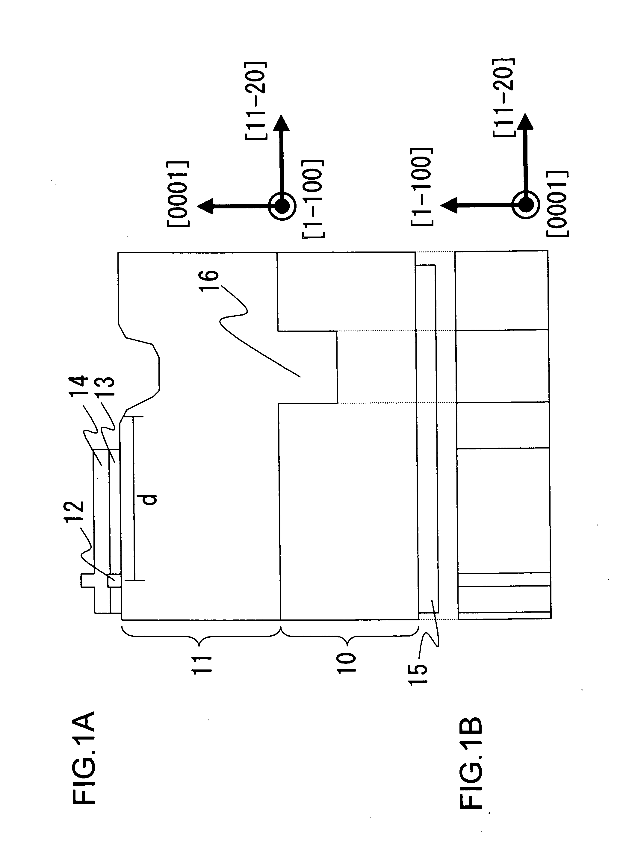
A nitride semiconductor laser device uses a substrate with low defect density, contains reduced strains inside a nitride semiconductor film, and thus offers a satisfactorily long useful life. On a GaN substrate (10) with a defect density as low as 106 cm−2 or less, a stripe-shaped depressed portion (16) is formed by etching. On this substrate (10), a nitride semiconductor film (11) is grown, and a laser stripe (12) is formed off the area right above the depressed portion (16). With this structure, the laser stripe (12) is free from strains, and the semiconductor laser device offers a long useful life. Moreover, the nitride semiconductor film (11) develops reduced cracks, resulting in a greatly increased yield rate.
Description
[0001] This nonprovisional application claims priority under 35 U.S.C. § 119(a) on Patent Applications Nos. 2003-204262 and 2004-183163 filed in Japan on Jul. 31, 2003 and Jun. 22, 2004, respectively, the entire contents of which are hereby incorporated by reference. BACKGROUND OF THE INVENTION [0002] 1. Field of the Invention [0003] The present invention relates to a nitride semiconductor light-emitting device, and to a method for fabricating one. More particularly, the present invention relates to a nitride semiconductor light-emitting device that uses a nitride semiconductor as a substrate thereof [0004] 2. Description of Related Art [0005] There have been fabricated prototypes of semiconductor laser devices that oscillate in a region ranging from ultraviolet to visible light by the use of a nitride semiconductor material as exemplified by GaN, AlN, InN, and composite crystals thereof. For such purposes, GaN substrates are typically used, and therefore GaN substrates have been in...
Claims
Login to View More Application Information
Patent Timeline
 IPC IPC(8): H01S5/343H01S5/00H01S5/02H01S5/22H01S5/223
CPCB82Y20/00H01L33/007H01S5/0213H01S5/2201H01S2304/12H01S5/2231H01S5/34333H01S2304/04H01S5/2214
InventorKAMIKAWA, TAKESHIYAMADA, EIJIARAKI, MASAHIROKANEKO, YOSHIKA
OwnerSHARP FUKUYAMA LASER CO LTD