
Growth of AsSb-Based Semiconductor Structures on InP Substrates Using Sb-Containing Buffer Layers

Inactive Publication Date: 2008-09-11
THE BOARD OF TRUSTEES OF THE UNIV OF ILLINOIS
View PDF13 Cites 4 Cited by
  • Summary
  • Abstract
  • Description
  • Claims
  • Application Information

AI Technical Summary

Benefits of technology

[0007]This invention provides an improved method for preparing high quality and low defect density Sb-containing alloys on lattice-mismatched substrates using Sb-containing buffer layers.

Problems solved by technology

The substrate and desired semiconductor are lattice-mismatched.

Method used


Image

  • Growth of AsSb-Based Semiconductor Structures on InP Substrates Using Sb-Containing Buffer Layers
  • Growth of AsSb-Based Semiconductor Structures on InP Substrates Using Sb-Containing Buffer Layers
  • Growth of AsSb-Based Semiconductor Structures on InP Substrates Using Sb-Containing Buffer Layers

Examples


experiment two

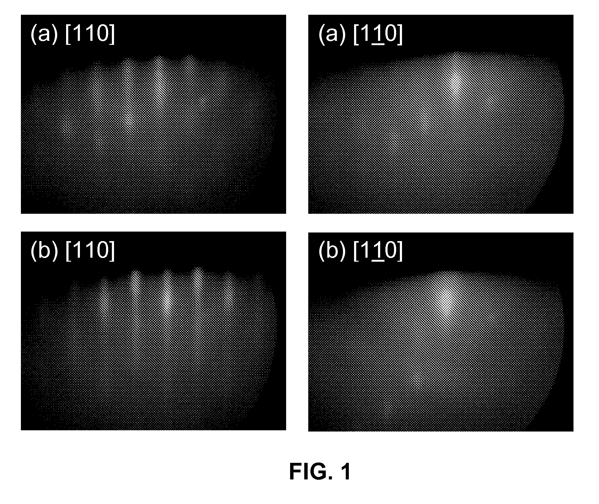
[0041]The epitaxial growth was carried out in a gas-source molecular beam epitaxy system. Arsine (AsH3) and phosphine (PH3) injected though high temperature crackers were used to generate As2 and P2, respectively. Mass flow controllers were used to adjust the flows of these two gases. Antimony molecular beam was supplied by thermally decomposing high purity antimony into Sb2 via an antimony valved cracker. The Sb2 flux was precisely controlled by a needle valve located at the front of the valved cracker. The substrate temperature was controlled and monitored by a thermal couple in contact with the backside of the sample holder. A pyrometer aiming at the center of the sample was used to measure the substrate temperature through a quartz view port on the growth chamber. During the growth, the RHEED patterns were used to monitor the status of the surface reconstructions.

[0042]Two-inch diameter epi-ready semi-insulating (001) InP substrates were cut into quarters and mounted on molybden...


PUM


Abstract

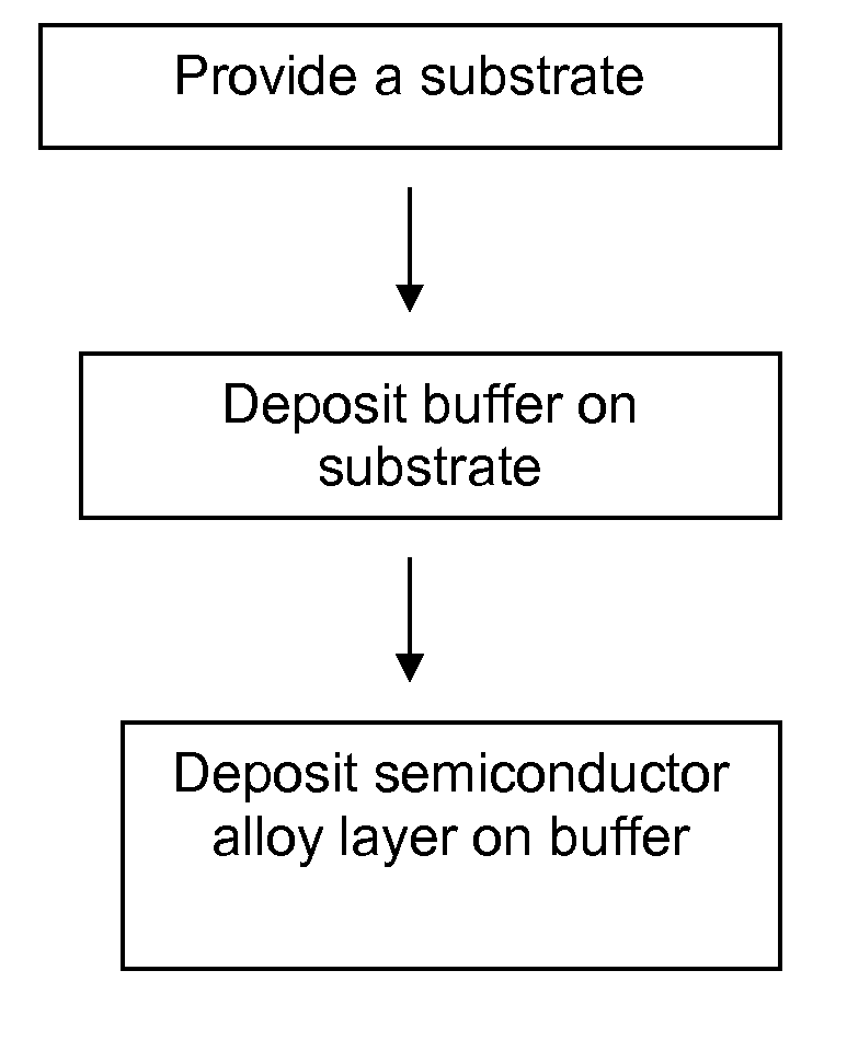
This invention provides high quality and low defect density Sb-containing alloys on lattice-mismatched substrates using Sb-containing buffer layers. More specifically, provided is a method of forming an epitaxial semiconductor alloy on a substrate, comprising: providing a substrate (such as InP); growing an Sb-containing buffer layer on the substrate; and growing a layer of As / Sb-containing semiconductor alloy on the buffer layer.

Description

CROSS-REFERENCE TO RELATED APPLICATIONS[0001]This application claims priority from U.S. provisional application No. 60 / 862,690, filed Oct. 24, 2006, which is hereby incorporated by reference to the extent not inconsistent with the disclosure herewith.STATEMENT REGARDING FEDERALLY SPONSORED RESEARCH OR DEVELOPMENT[0002]This invention was made with U.S. government support under grant number HR0011-04-0034 awarded by Defense Advanced Research Projects Agency / Microsystems Technology Office. The U.S. government has certain rights in the invention.BACKGROUND OF THE INVENTION[0003]Compound semiconductors with lattice constant around 6.1 Å have drawn much attention in recent years. The 6.1 Å binary alloy family includes InAs, GaSb, and AlSb, which have the lattice constants of 6.058 Å, 6.096 Å, and 6.136 Å, respectively. In addition to the binary alloys, ternary, quaternary and higher complexity semiconductor materials are desirable. Transport devices such as high electron mobility transist...

Claims


Application Information

Patent Timeline
IPC IPC(8): H01L29/267H01L21/205
CPCC30B23/02C30B23/025C30B29/40H01L21/02381H01L21/02461H01L29/778H01L21/02466H01L21/02505H01L21/02549H01L29/205H01L21/02463
Inventor CHENG, KEH-YUNGWU, BING-RUEY
Owner THE BOARD OF TRUSTEES OF THE UNIV OF ILLINOIS
Learn More