Semiconductor stacking structure, and method and apparatus for separating nitride semiconductor layer using same

Active Publication Date: 2017-09-21
SAMSUNG ELECTRONICS CO LTD
View PDF9 Cites 4 Cited by
  • Summary
  • Abstract
  • Description
  • Claims
  • Application Information

AI Technical Summary

Benefits of technology

The present patent proposes a new method and apparatus for separating a nitride semiconductor layer from a substrate using a mechanical force without the need for an expensive laser device. An inorganic thin film containing cavities is formed between the substrate and the nitride semiconductor layer, allowing for easy separation without any deterioration caused by the laser. This method and apparatus result in higher production efficiency and lower defect density in the nitride semiconductor layer, leading to better quality LEDs and greater reliability. Additionally, a new mechanism is proposed for the separation process.

Problems solved by technology

However, because these heterogeneous substrate materials have a lattice constant mismatch and a difference in thermal expansion coefficient with nitride, a nitride semiconductor layer grown on the heterogeneous substrate includes many crystal defects such as dislocation.
The defect acts as a key factor that degrades the performance of nitride semiconductor devices such as LEDs.
The use of a thick substrate only contributes to the reduced superficial phenomenon, and is not technology that reduces the stress of a thin film itself.
However, even though a laser lift-off process is used, substrate warpage occurs due to a difference in thermal expansion coefficient between a sapphire substrate and nitride semiconductor, or a nitride semiconductor layer is melted using a laser and peeled off, so a side effect is the occurrence of thermal stress during the process due to high temperature heat at a local area.
Due to laser beam impacts, the nitride semiconductor layer is susceptible to defects such as cracks and the nitride semiconductor layer may be damaged, and further, the nitride semiconductor layer is prone to breakage, and thus, the process is unstable.

Method used


Image

  • Semiconductor stacking structure, and method and apparatus for separating nitride semiconductor layer using same
  • Semiconductor stacking structure, and method and apparatus for separating nitride semiconductor layer using same
  • Semiconductor stacking structure, and method and apparatus for separating nitride semiconductor layer using same

Examples


Embodiment Construction

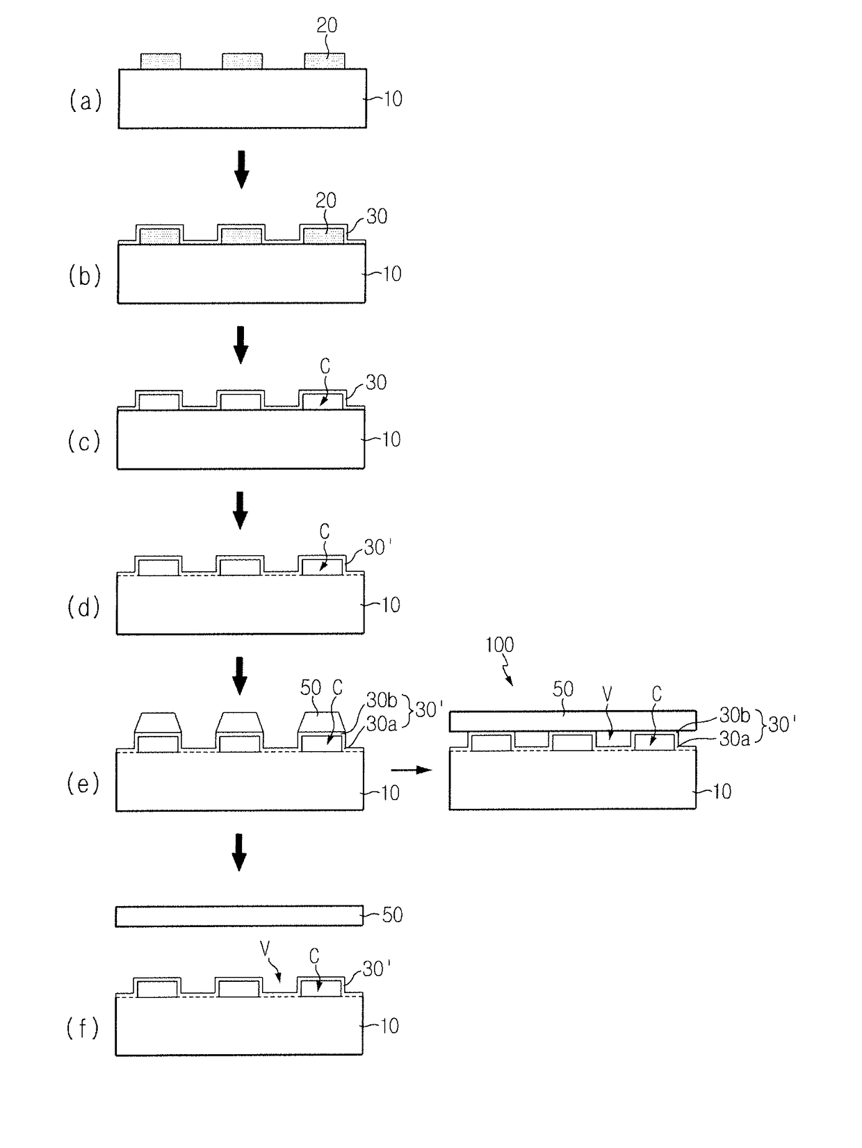
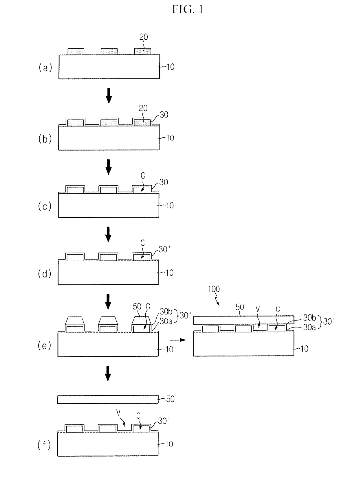
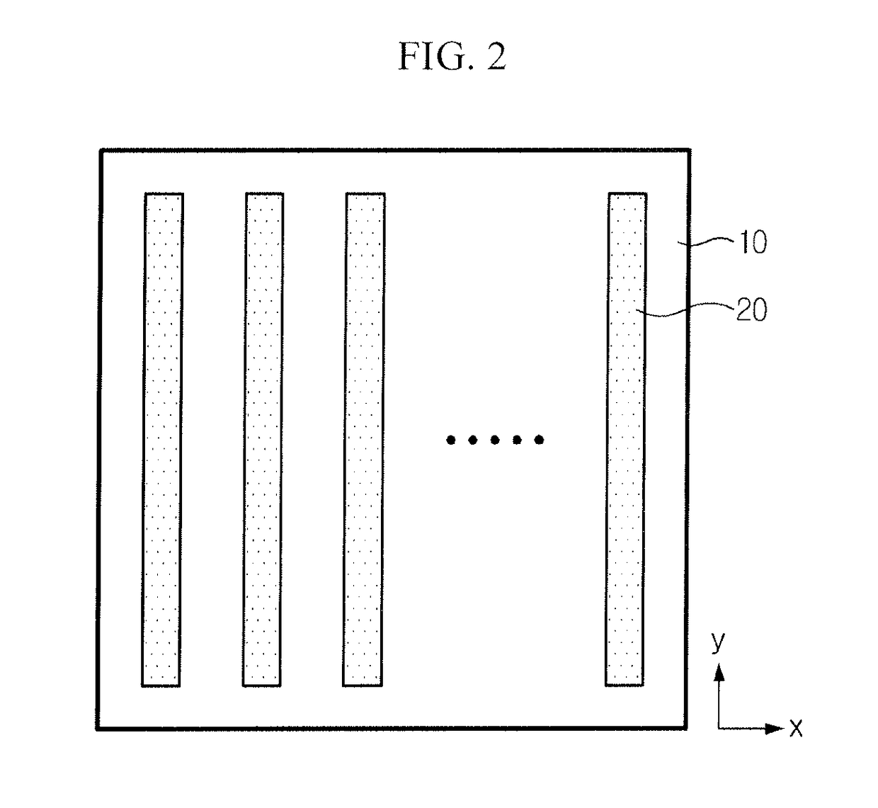
[0049]Hereinafter, the present disclosure will be described in further detail with reference to the accompanying drawings. The embodiments described hereinafter may be modified in many different forms, and the scope of the present disclosure is not limited to the following embodiments. The embodiments of the present disclosure are provided to help persons having ordinary skill in the art understand the present disclosure completely and fully. Accordingly, the shape of the elements in the drawings is exaggerated for clarity, and elements indicated by the same symbol in the drawings represent the same element.

[0050]The inventors have proposed various research results for relieving stress of a nitride semiconductor layer by forming cavities on a substrate of heterogeneous material, growing a nitride semiconductor layer, and deforming the cavities. This application is based on the research results of a method for manufacturing a LED or a nitride semiconductor free-standing or nitride se...


PUM


Abstract

A semiconductor stacking structure according to the present invention comprises: a monocrystalline substrate which is disparate from a nitride semiconductor; an inorganic thin film which is formed on a substrate to define a cavity between the inorganic thin film and the substrate, wherein at least a portion of the inorganic thin film is crystallized with a crystal structure that is the same as the substrate; and a nitride semiconductor layer which is grown from a crystallized inorganic thin film above the cavity. The method and apparatus for separating a nitride semiconductor layer according the present invention mechanically separate between the substrate and the nitride semiconductor layer. The mechanical separation can be performed by a method of separation of applying a vertical force to the substrate and the nitride semiconductor layer, a method of separation of applying a horizontal force, a method of separation of applying a force of a relative circular motion, and a combination thereof.

Description

TECHNICAL FIELD[0001]The present disclosure relates to a semiconductor layer of gallium nitride (GaN) or mixed nitride of gallium and other metal and its formation method. Furthermore, the present disclosure relates to an electronic or opto-electronic device including the layer, a nitride semiconductor substrate and its manufacturing method. The technical field of the present disclosure may be, in broad senses, defined as a semiconductor stacking structure for forming a nitride semiconductor layer with few crystal defects and high quality on a substrate and its formation method.BACKGROUND ART[0002]Nitride semiconductor of elements in Group III or V in the periodic table occupies an important position in the field of electronic and opto-electronic devices, and this field will be more important in the future. In practice, nitride semiconductor has a wide range of applications, ranging from laser diodes (LDs) to transistors that can operate at high frequency and high temperature. Furth...

Claims


Application Information

Patent Timeline
IPC IPC(8): H01L33/12H01L33/00H01L33/32
CPCH01L33/12H01L33/0079H01L33/007H01L33/32H01L33/22H01L21/0242H01L21/02433H01L21/02488H01L21/02513H01L21/0254H01L21/02639H01L21/0265H01L21/67092H01L33/0093
Inventor YOON, EUI-JOONMOON, DAE-YOUNGJANG, JEONG-HWANPARK, YONGJOBAE, DUK-KYU
Owner SAMSUNG ELECTRONICS CO LTD
Why Eureka
Try Eureka