Sos substrate having low surface defect density

Inactive Publication Date: 2012-05-17
SHIN ETSU CHEM IND CO LTD
View PDF2 Cites 18 Cited by
  • Summary
  • Abstract
  • Description
  • Claims
  • Application Information

AI Technical Summary

Benefits of technology

[0010]In view of the current circumstances, an object of the invention is to solve a problem that a defect density increases

Problems solved by technology

However, use of the heteroepitaxial SOS substrate is limited to small individual parts, such as a switch, at present since a defect density is high.
However, even if the double solid phase growth method is used, the defect density is about 106 to 107 pieces / cm2 so that it is difficult to make a recent highly downscaled and sophisticated device.
Further, it is also difficult to make a relatively large size device such as a system chip having many functions.
It can be said that this is due to an essential problem of the heteroepitaxial growth (an epitaxial growth of materials having different lattice constants).

Method used


Image

  • Sos substrate having low surface defect density
  • Sos substrate having low surface defect density
  • Sos substrate having low surface defect density

Examples


example 1

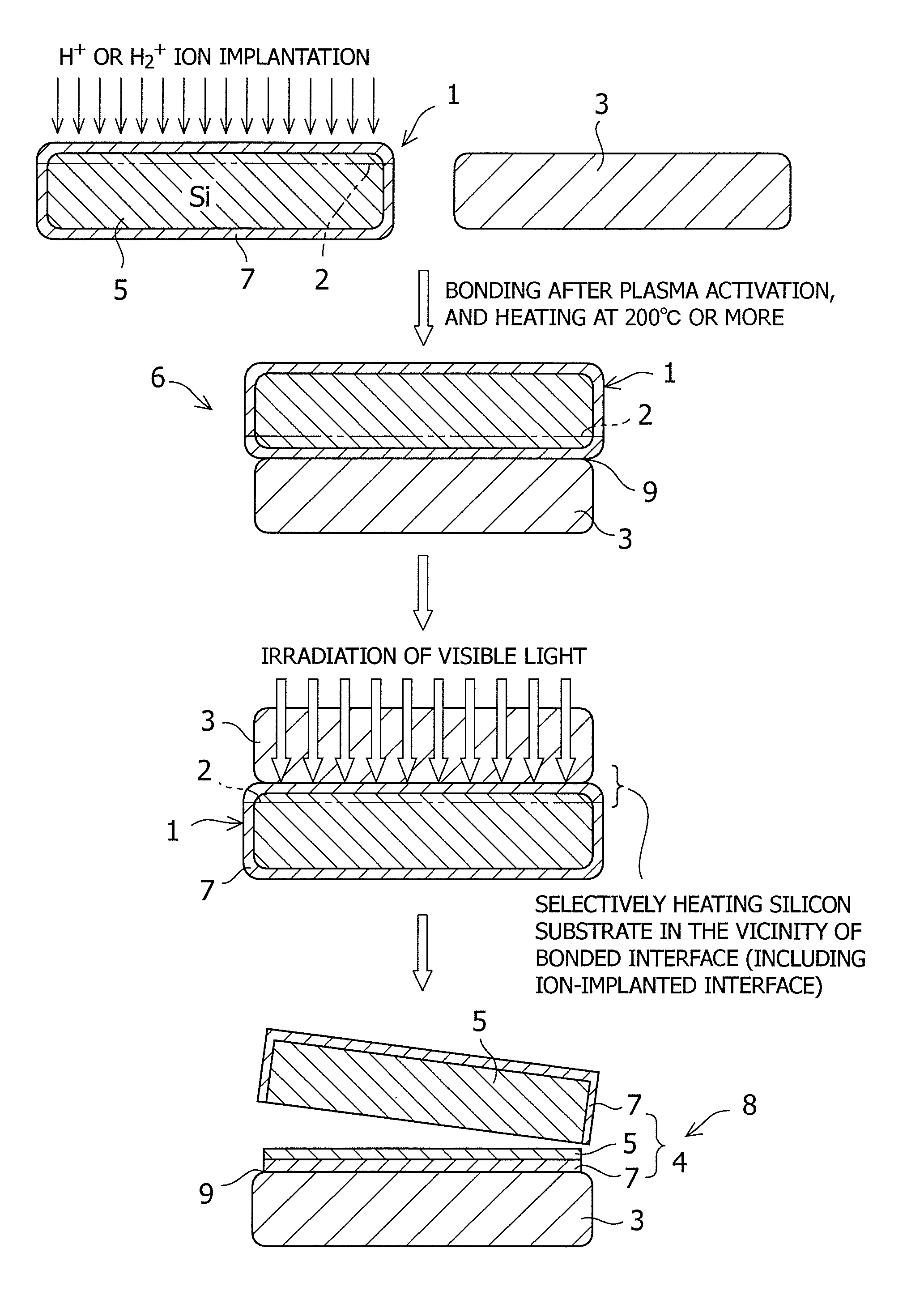
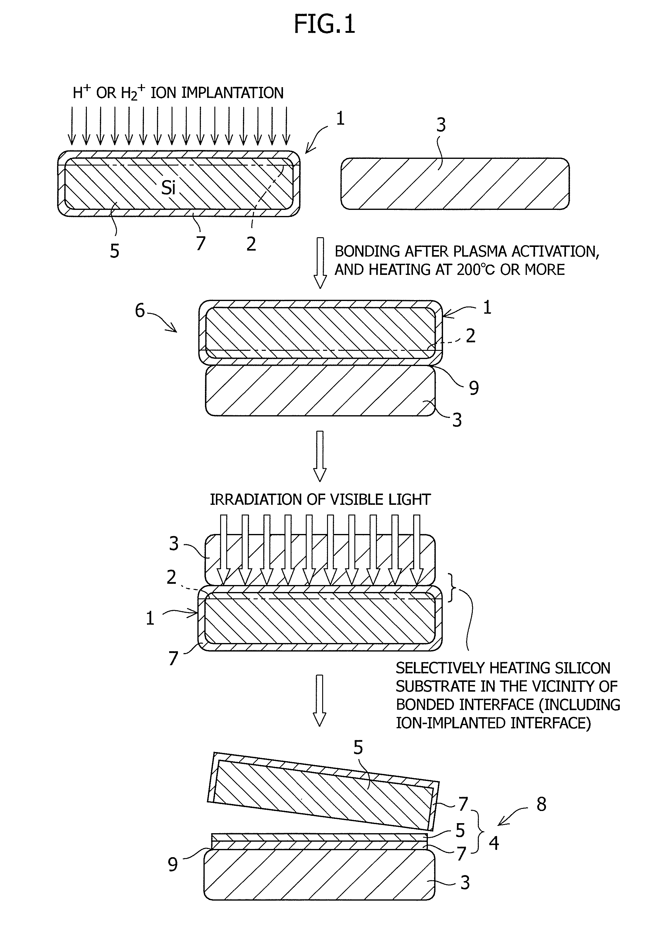
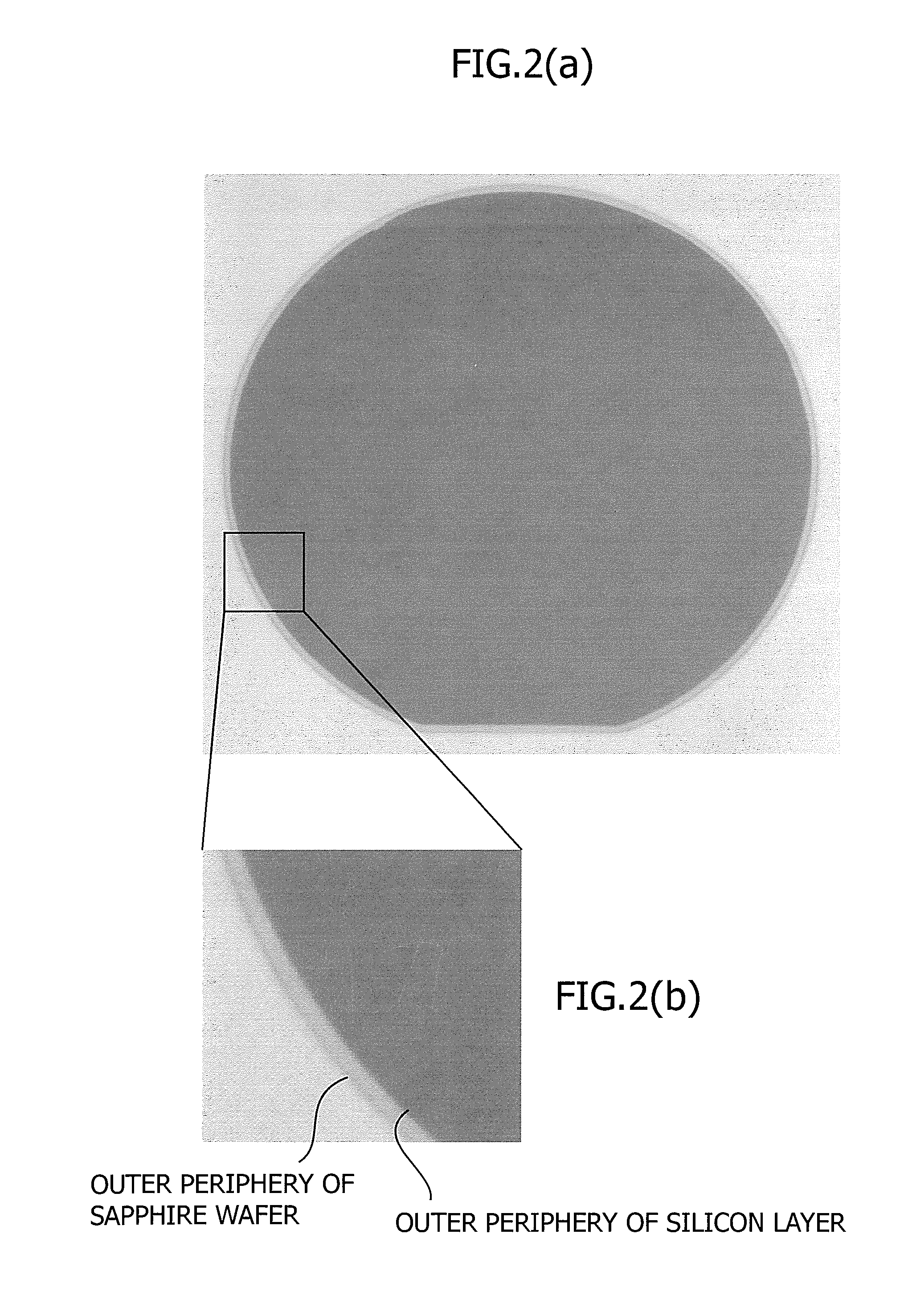
[0070]A silicon substrate (thickness 625 μm) having a diameter of 150 mm on which an oxide film had been grown to 200 nm was subjected to implantation of hydrogen ions at 57 keV and a dose amount of 6.0×10¹⁶ atoms / cm2. Both surfaces of a sapphire substrate were subjected to ion beam activation treatment. Then the silicon substrate was bonded to the sapphire substrate at 150° C. After the bonded substrates were subjected to heat treatment at 225° C. for 24 hours for primary bonding, a green laser having a wavelength of 532 nm was irradiated from the sapphire substrate side at 200° C. A laser condition at the time was 20 J / cm2. After the overall surface of the substrate was irradiated, a silicon film was transferred to the sapphire substrate by splitting along the bonded interface to which a mechanical impact was applied. The transfer of the silicon film onto the overall surface of the sapphire substrate could be confirmed. After the silicon layer of the substrate was made to a thickn...

example 2

[0071]A silicon substrate (thickness 625 μm) having a diameter of 150 mm on which an oxide film had been grown to 200 nm was subjected to implantation of hydrogen ions at 57 keV and a dose amount of 6.0×10¹⁶ atoms / cm2. Both surfaces of a sapphire substrate were subjected to plasma activation treatment. Then the silicon substrate was bonded to the sapphire substrate at 200° C. After the bonded substrates were subjected to heat treatment at 225° C. for 24 hours for primary bonding, light from a xenon plash lamp was irradiated from the sapphire substrate side at 250° C. After the overall surface of the substrate was irradiated, a silicon film was transferred to the sapphire substrate by splitting along a bonded interface to which a mechanical impact was applied. The transfer of the silicon film onto the overall surface of the sapphire substrate could be confirmed. After the silicon layer of the substrate was made to a thickness of 200 nm by etching (an ammonia hydrogen peroxide solutio...

example 3

[0073]A silicon substrate (thickness 625 μm) having a diameter of 150 mm on which an oxide film had been grown to 200 nm was subjected to implantation of hydrogen ions at 57 keV and a dose amount of 6.0×10¹⁶ atoms / cm2. Both surfaces of a sapphire substrate were subjected to UV ozone activation treatment. Then, the silicon substrate was bonded to the sapphire substrate at 100° C. After the bonded substrates were subjected to heat treatment at 225° C. for 24 hours for primary bonding, light from a xenon flash lamp were irradiated from the sapphire substrate side at 175° C. After the overall surface of the substrate was irradiated, a silicon film was transferred to the sapphire substrate by splitting along a bonded interface to which a mechanical impact is applied. The film thickness was made to about 250 nm by EDP polishing and CMP polishing. Since splitting and transferring were regulated by an ion implanted interface, the film thickness variation after the transfer was suppressed to...


PUM


Abstract

A method of making bonded SOS substrate with a semiconductor film on or above a sapphire substrate by implanting ions from a surface of the semiconductor substrate to form an ion-implanted layer; activating at least a surface of one of the sapphire substrate and the semiconductor substrate from which the ions have been implanted; bonding the surface of the semiconductor substrate and the surface of the sapphire substrate at a temperature of from 50° C. to 350° C.; heating the bonded substrates at a maximum temperature of from 200° C. to 350° C.; and irradiating visible light from a sapphire substrate side or a semiconductor substrate side to the ion-implanted layer of the semiconductor substrate to make the interface of the ion-implanted layer brittle at a temperature of the bonded body higher than the temperature at which the surfaces were bonded, to transfer the semiconductor film to the sapphire substrate.

Description

BACKGROUND OF THE INVENTION[0001]1. Field of the Invention[0002]The invention relates to a silicon-on-sapphire SOS substrate having a low surface defect density.[0003]2. Description of Related Art[0004]Conventionally, a silicon-on-sapphire (SOS) substrate containing sapphire having a high insulation property, a low dielectric loss and a high thermal conductivity as a handle substrate has come into practical use since 1960s. The SOS substrate is an oldest silicon-on-insulator (SOI) substrate and forms an SOI structure by heteroepitaxially growing silicon on an R surface (1012) of sapphire.[0005]However, recently, an SOI using a SIMOX method, the bonding method and the like has become a main stream. Although an SOS substrate, which is a SOI substrate having silicon on a sapphire substrate, cannot cope, the SOS substrate has been used only for a device such as a high frequency device requiring a low dielectric loss. It is known that since a heteroepitaxial SOS substrate is formed by he...

Claims


Application Information

Patent Timeline
IPC IPC(8): H01L21/762H01L29/02
CPCH01L21/265H01L21/76254H01L21/268H01L21/26506H01L21/2658
Inventor AKIYAMA, SHOJIITO, ATSUOTOBISAKA, YUJIKAWAI, MAKOTO
Owner SHIN ETSU CHEM IND CO LTD
Why Eureka
Try Eureka