Sic epitaxial wafer and method for producing same

Active Publication Date: 2020-03-12
SHOWA DENKO KK +2
View PDF0 Cites 1 Cited by
  • Summary
  • Abstract
  • Description
  • Claims
  • Application Information

AI Technical Summary

Benefits of technology

The present invention is a SiC epitaxial wafer which has a low dislocation defect density on the basal plane, which affects the operation of SiC devices. It also results in a high yield and quality of devices.

Problems solved by technology

On the other hand, part of basal plane dislocations, which continues from the SiC single crystal substrate to the epitaxial layer as it is, is resulted in a device killer defect.
In step flow growth, it is known that when a foreign matter such as a two-dimensional nucleus is generated on a terrace, the lateral growth of atomic steps is disturbed and crystal defects are generated.
In addition, in Patent Document 3, it is disclosed that adhesion of Si droplets (silicon droplets) is considered to cause high-density abnormal growth nucleus.

Method used


Image

  • Sic epitaxial wafer and method for producing same
  • Sic epitaxial wafer and method for producing same
  • Sic epitaxial wafer and method for producing same

Examples


example 1

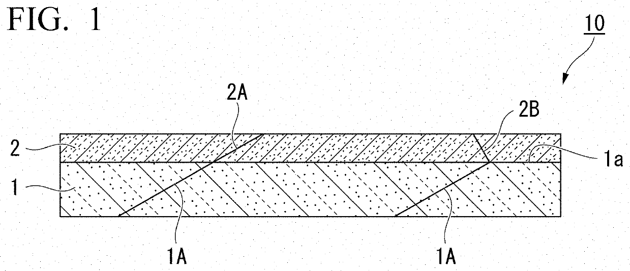
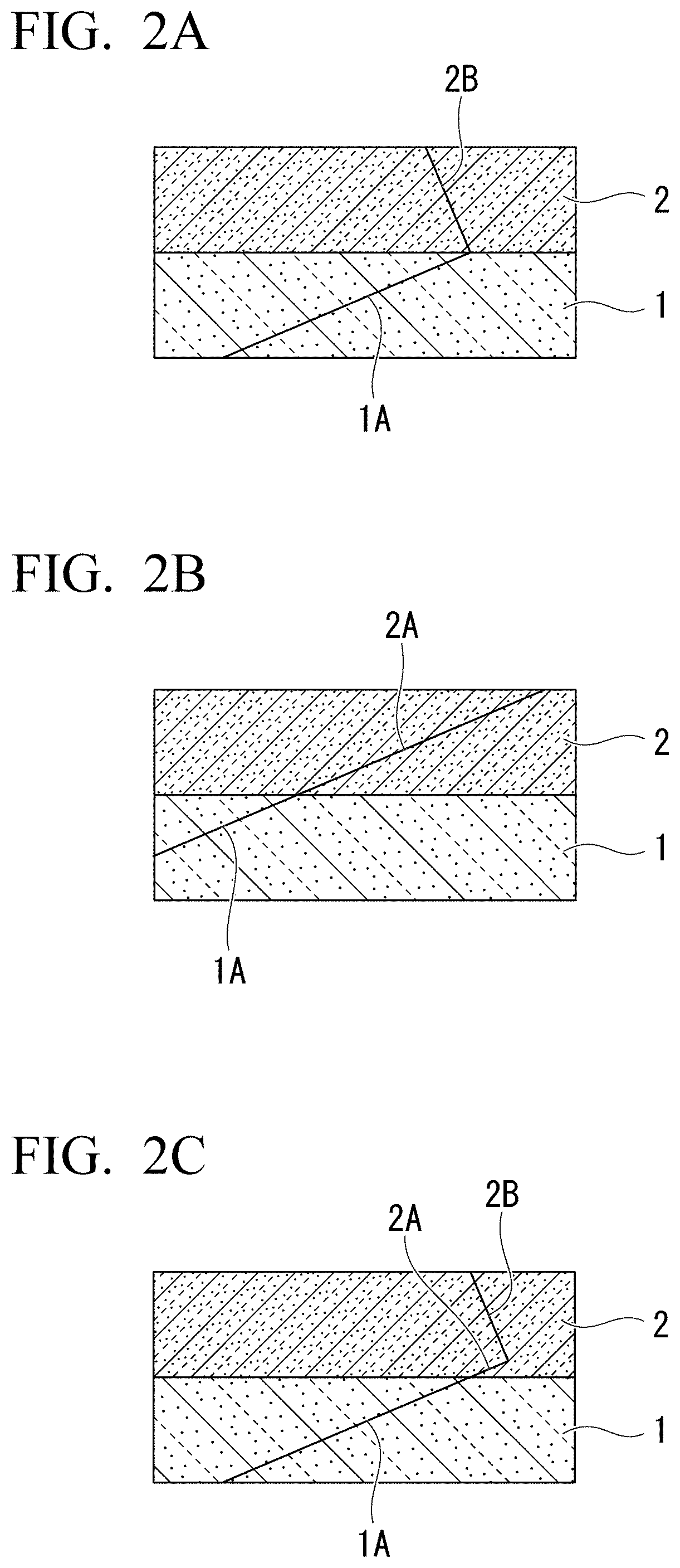
[0138]A 6-inch SiC single crystal substrate was prepared. The prepared SiC single crystal substrate is a 4H polytype, and a main surface thereof includes an Si surface having an offset-angle of 4° in direction from (0001) plane.

[0139]Next, the SiC single crystal substrate was introduced into a growth furnace, and a cleaning step of performing gas etching on a growth surface using hydrogen gas was performed. An etching temperature was set to 1600° C. same as the epitaxial growth temperature, and the pressure was set to 30 torr.

[0140]Next, while supplying hydrogen to the surface of the etched 4H-SiC single crystal substrate and maintaining the same pressure, feeding of trichlorosilane and propane as raw material gases and HCl as a gas containing Cl element was started at the same time to grow an epitaxial layer.

[0141]In the epitaxial growth step, the ratio of the C-based raw material gas to the Si-based raw material gas was set to the C / Si ratio of 1.0, and the gas flow rate was set ...

example 2

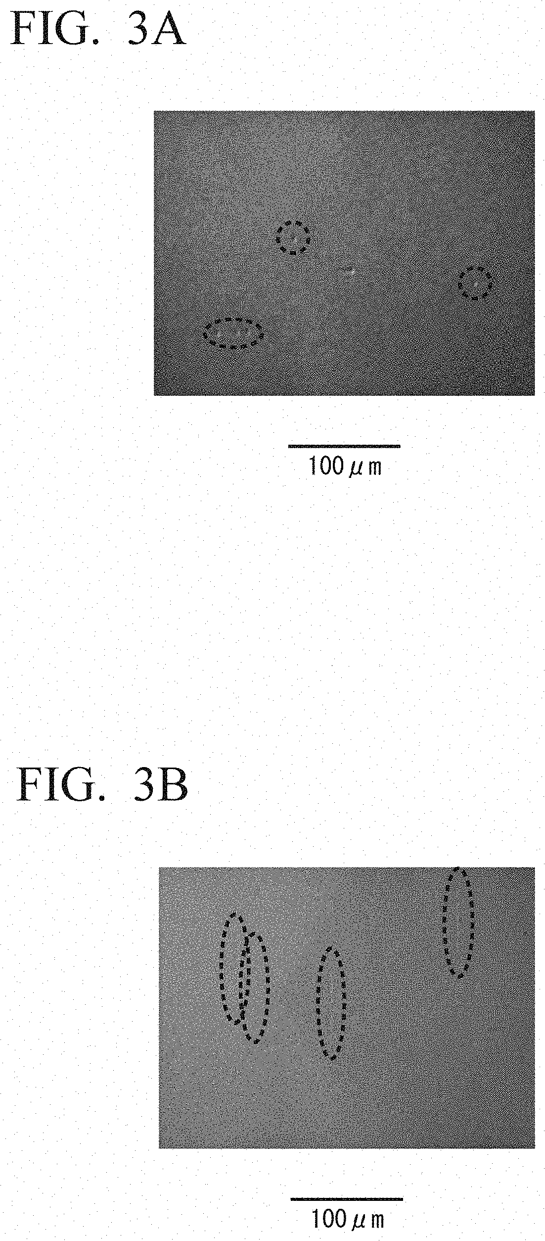
[0144]Example 2 was the same as Example 1 except that the Cl / Si ratio was set to 10. The basal plane dislocation density of the obtained SiC epitaxial wafer was evaluated. The basal plane dislocations were 0.04 dislocations / cm2, and there were no pits caused by Si droplets.

example 3

[0145]Example 3 was the same as Example 1 except that the growth rate was set to 65 μm / h. The basal plane dislocation density of the obtained SiC epitaxial wafer was evaluated. The basal plane dislocations were 0.01 dislocations / cm2, and pits caused by Si droplets were 0.053 pits / cm2.


PUM

PropertyMeasurementUnit
Temperatureaaaaaaaaaa
Pressureaaaaaaaaaa

Abstract

A method for producing a SiC epitaxial wafer according to the present embodiment includes: an epitaxial growth step of growing the epitaxial layer on the SiC single crystal substrate by feeding an Si-based raw material gas, a C-based raw material gas, and a gas including a Cl element to a surface of a SiC single crystal substrate, in which the epitaxial growth step is performed under growth conditions that a film deposition pressure is 30 torr or less, a Cl / Si ratio is in a range of 8 to 12, a C / Si ratio is in a range of 0.8 to 1.2, and a growth rate is 50 μm / h or more from an initial growth stage.

Description

TECHNICAL FIELD[0001]The present invention relates to a SiC epitaxial wafer and a method for producing the same.[0002]Priority is claimed on Japanese Patent Application No. 2017-104625, filed on May 26, 2017, the content of which is incorporated herein by reference.BACKGROUND ART[0003]Silicon carbide (SiC) has features such that a dielectric breakdown field is larger by one order of magnitude, a band gap is three times larger, and a thermal conductivity is approximately three times higher than those of silicon (Si). Therefore, application of silicon carbide (SiC) to power devices, high-frequency devices, high-temperature operation devices, and the like is expected.[0004]In order to promote the practical application of SiC devices, it is essential to establish techniques for high-quality epitaxial growth and high-quality SiC epitaxial wafers.[0005]The SiC device is prepared by using a SiC epitaxial wafer wherein an epitaxial layer (film) to be an active region of the device is grown ...

Claims


Application Information

Patent Timeline
IPC IPC(8): H01L29/16C23C16/42C30B29/36H01L21/02
CPCC30B29/36H01L21/02529C23C16/42H01L29/1608C23C16/325C30B25/165C30B25/20H01L21/02378H01L21/02433H01L21/02576H01L21/02579H01L21/0262H01L21/02661
Inventor FUKADA, KEISUKEISHIBASHI, NAOTOBANDO, AKIRAITO, MASAHIKOKAMATA, ISAHOTSUCHIDA, HIDEKAZUHARA, KAZUKUNINAITO, MASAMIUEHIGASHI, HIDEYUKIFUJIBAYASHI, HIROAKIAOKI, HIROFUMISUGIURA, TOSHIKAZUSUZUKI, KATSUMI
Owner SHOWA DENKO KK
Why Eureka
Try Eureka