Laser device integrated with semiconductor optical amplifier on silicon substrate

Active Publication Date: 2018-03-29
SAMSUNG ELECTRONICS CO LTD
View PDF0 Cites 12 Cited by
  • Summary
  • Abstract
  • Description
  • Claims
  • Application Information

AI Technical Summary

Benefits of technology

The patent text describes a laser device that includes a semiconductor material on a silicon substrate. The device includes a laser cavity with a first active region and a second active region, and a semiconductor op amplifier integrated with the laser cavity. The device generates light with a low defect density and has improved performance compared to traditional laser devices. The technical effects of the patent text include improved laser efficiency, reduced light absorption, and improved wavelength control.

Problems solved by technology

However, the laser devices that have been developed so far have limitations regarding the lifetime, output, and reliability because of defects caused by a difference in a lattice constant between the silicon substrate and the group III-V compound semiconductor.
However, when a laser device of this wavelength band is formed of the group III-V compound semiconductor, more defects typically occur than when light having other wavelength bands is used.

Method used


Image

  • Laser device integrated with semiconductor optical amplifier on silicon substrate
  • Laser device integrated with semiconductor optical amplifier on silicon substrate
  • Laser device integrated with semiconductor optical amplifier on silicon substrate

Examples


Embodiment Construction

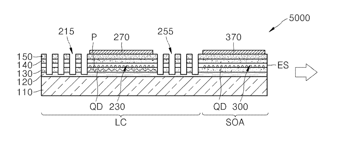
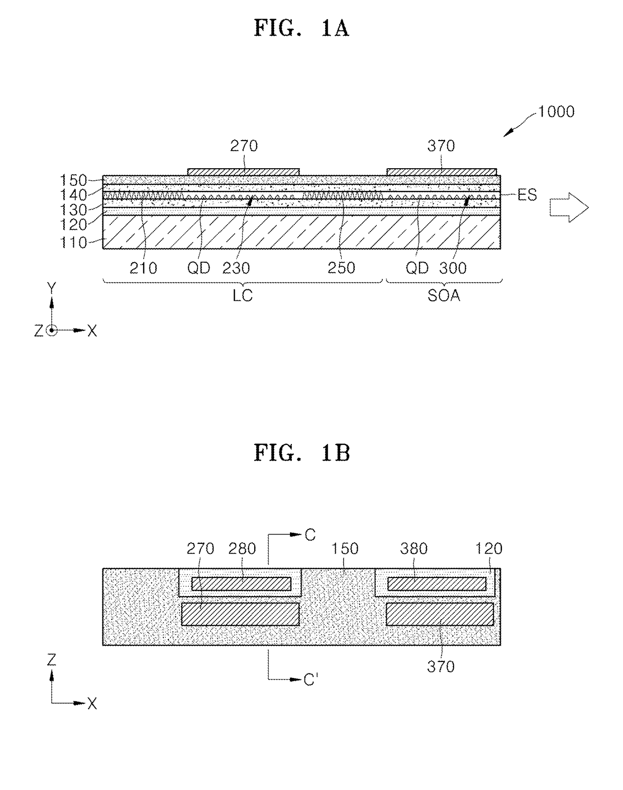
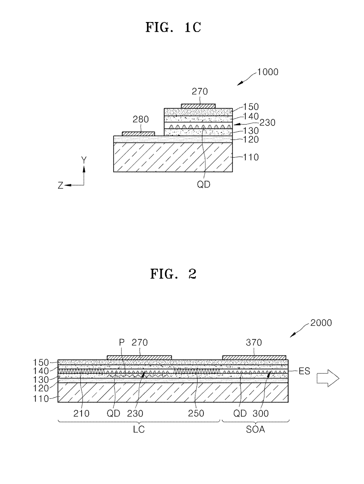
[0043]As used herein, the term “and / or” includes any and all combinations of one or more of the associated listed items. Expressions such as “at least one of,” when preceding a list of elements, modify the entire list of elements and do not modify the individual elements of the list.

[0044]As the invention allows for various changes and numerous embodiments, particular embodiments will be illustrated in the drawings and described in detail in the written description. The advantages and features of the present invention and methods of achieving the advantages and features will be described more fully with reference to the accompanying drawings, in which exemplary embodiments of the invention are shown. The invention may, however, be embodied in many different forms and should not be construed as being limited to the embodiments set forth herein; rather these embodiments are provided so that this disclosure will be thorough and complete, and will fully convey the concept of the inventi...


PUM


Abstract

A laser device includes a silicon substrate, a buffer layer on the silicon substrate, a laser cavity on the buffer layer including a first active region based on group III-V semiconductor quantum dots, and a semiconductor optical amplifier that is integrated with the laser cavity on the buffer layer, includes a second active region based on group III-V semiconductor quantum dots, and amplifies light emitted from the laser cavity.

Description

RELATED APPLICATIONS[0001]This application claims priority from Korean Patent Application No. 10-2014-0018655, filed on Feb. 18, 2014, in the Korean Intellectual Property Office, the disclosure of which is incorporated herein in its entirety by reference.BACKGROUND1. Field[0002]Example embodiments relate to laser devices, and / or to laser devices formed of a group III-V-based semiconductor material on a silicon substrate, the group III-V-based semiconductor material having a low defect density.2. Description of the Related Art[0003]Interest in technologies for forming silicon-based photonic integrated circuits has recently increased. A silicon-based photonic integrated circuit may include various optical devices such as a light source, an optical waveguide, an optical modulator, an optical filter, and a photodetector, and may transmit a signal through optical interconnection. Optical interconnection is a technology of transmitting / receiving data by using light, and has less transmiss...

Claims


Application Information

Patent Timeline
IPC IPC(8): H01L29/267H01L21/02H01S5/02H01S5/30H01S5/34
CPCH01S5/026H01S5/028H01S5/0625H01S5/1209H01S5/0287H01S5/06256H01S5/0265H01S5/0085H01S5/021H01S5/1039H01S5/125H01S5/3412H01S5/4012H01S5/4087H01S5/50H01S2301/173H01S5/04257G02B1/005H01S5/06808
Inventor KIM, TAEK
Owner SAMSUNG ELECTRONICS CO LTD
Why Eureka
Try Eureka