Strained Semiconductor FET Devices with Epitaxial Quality Improvement

Pending Publication Date: 2022-01-06
IBM CORP
View PDF5 Cites 0 Cited by
  • Summary
  • Abstract
  • Description
  • Claims
  • Application Information

AI Technical Summary

Benefits of technology

The present invention relates to strained semiconductor field-effect transistor (FET) devices and techniques for their formation using a spacer last process. The invention provides semiconductor FET devices with improved epitaxial quality and techniques for their formation using a sacrificial layer approach. The FET devices include source / drains that are offset from the gates, where the source / destinations are formed from an epitaxial material having low defect density that induces strain in the active layers. The gate spacers are formed from the same material as the inner spacers. The method for the invention involves forming sacrificial layers, recessing the sacrificial layers to form pockets, growing a sacrificial semiconductor material in the pockets, selectively removing the sacrificial semiconductor material, forming inner spacers, removing the sacrificial layers, and forming gates. The invention allows for improved strain in the active layers, which enhances device performance.

Problems solved by technology

However, it is difficult to grow the source and drain epitaxy with the inner spacers already in place.

Method used


Image

  • Strained Semiconductor FET Devices with Epitaxial Quality Improvement
  • Strained Semiconductor FET Devices with Epitaxial Quality Improvement
  • Strained Semiconductor FET Devices with Epitaxial Quality Improvement

Examples


Embodiment Construction

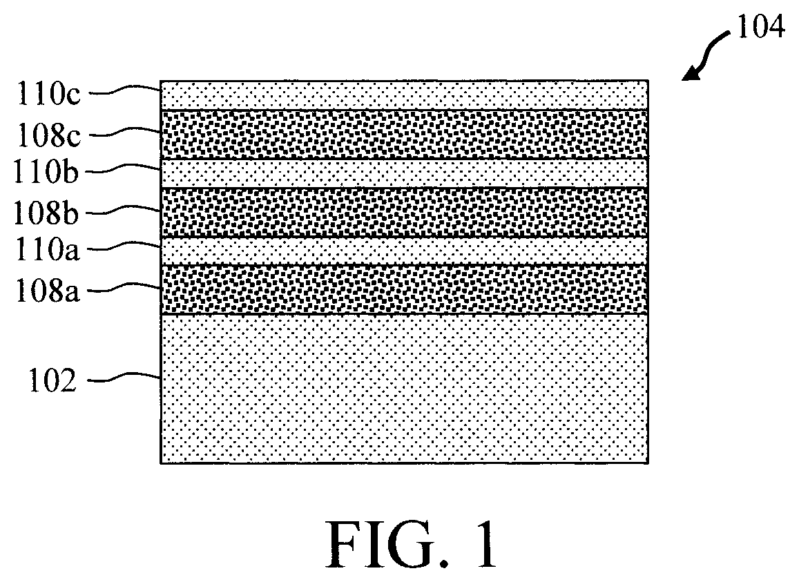
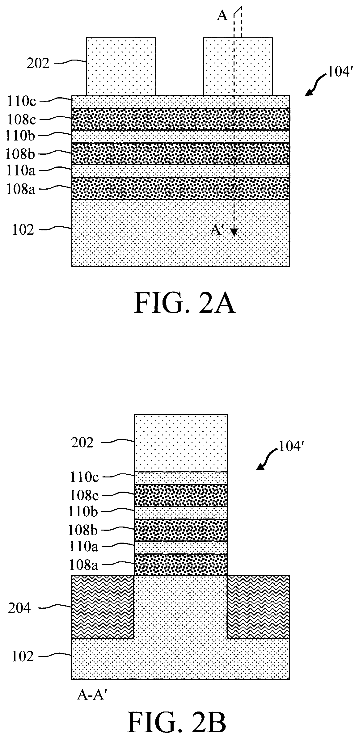
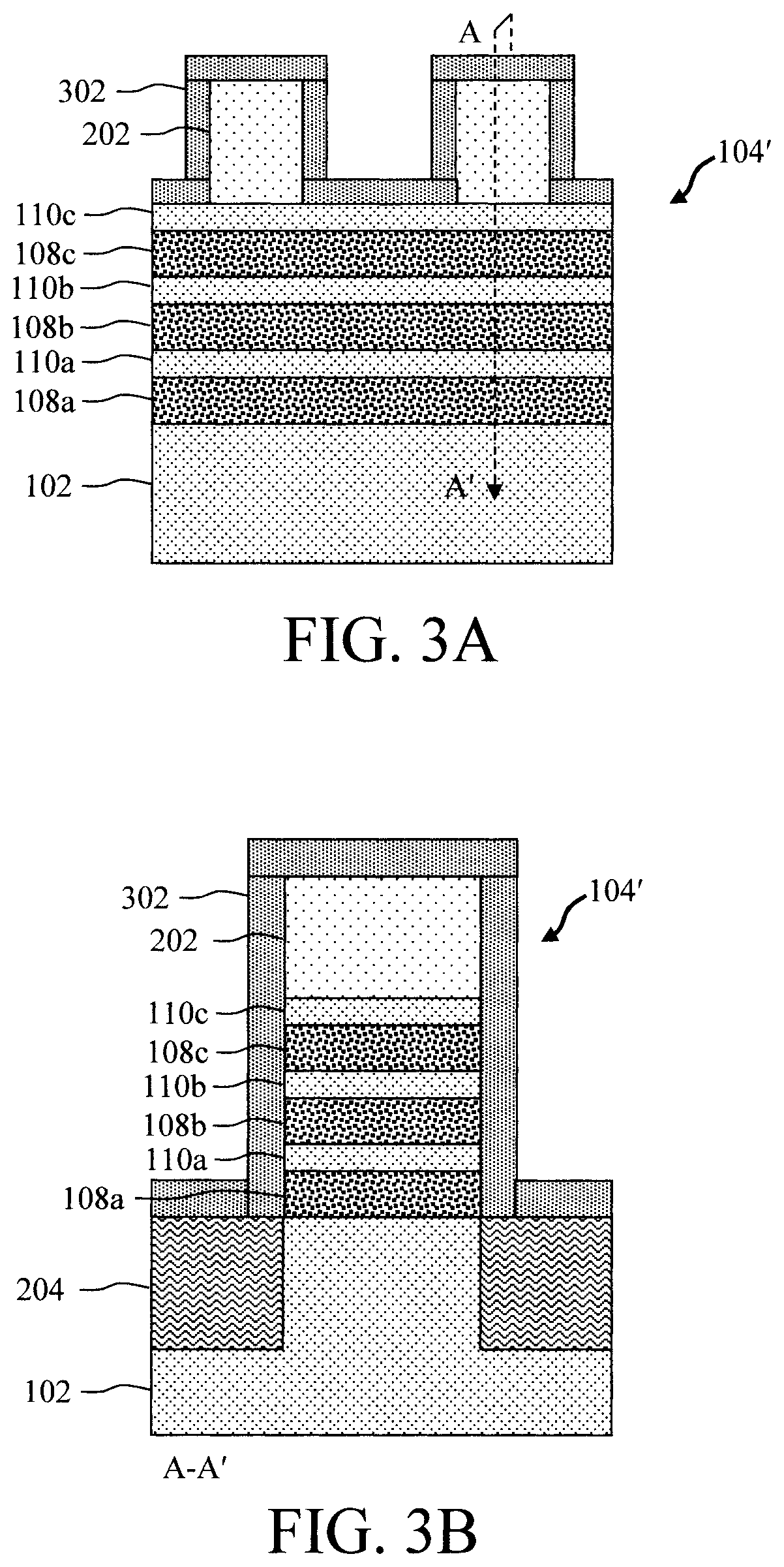
[0023]As provided above, nanosheet field-effect transistor (FET) device fabrication process flows where inner spacers are formed along the nanosheet stack prior to source and drain growth can present some notable drawbacks. For instance, there is only a small exposed area at the ends of the channel nanosheets for the source and drain epitaxy which makes the epitaxial growth process difficult.

[0024]Furthermore, the defectivity in the resulting source and drain epitaxy is high based on the different angle of epitaxy nucleation on the exposed ends of the channel nanosheets. With a high defectivity, there is almost no channel strain generated by the epitaxial material. Channel strain desirably enhances channel mobility and overall device performance.

[0025]Advantageously, provided herein are techniques for fabricating semiconductor FET devices such as nanosheet FET devices whereby the inner spacers are formed post epitaxial source / drain growth. By enabling the source / drain growth to occu...


PUM


Abstract

Strained semiconductor FET devices with epitaxial quality improvement are provided. In one aspect, a semiconductor FET device includes: a substrate; at least one device stack including active layers oriented horizontally one on top of another on the substrate; gates surrounding at least a portion of each of the active layers; gate spacers alongside the gates; and source / drains, interconnected by the active layers, on opposite sides of the gates, wherein the source / drains are offset from the gates by inner spacers, wherein the source / drains include an epitaxial material having a low defect density which induces strain in the active layers, and wherein the gate spacers are formed from a same material as the inner spacers. A method of forming the semiconductor FET device using a spacer last process is also provided.

Description

FIELD OF THE INVENTION[0001]The present invention relates to source / drain epitaxy in semiconductor field-effect transistor (FET) devices, and more particularly, to strained semiconductor FET devices with epitaxial quality improvement and techniques for formation thereof using a spacer-last process.BACKGROUND OF THE INVENTION[0002]A stacked nanosheet architecture is a promising design choice for the next generation of field-effect transistors (FETs). Advantageously, a nanosheet FET design enables the formation of gate-all-around or GAA configurations. With conventional process flows for nanosheet FET fabrication, inner spacers are formed along the nanosheet stack prior to source and drain growth. These inner spacers limit growth of the source and drain epitaxy to the ends of the channel nanosheets.[0003]However, it is difficult to grow the source and drain epitaxy with the inner spacers already in place. This is due to the small exposed area at the ends of the channel nanosheets. Fur...

Claims


Application Information

Patent Timeline
IPC IPC(8): H01L29/78H01L29/06H01L29/423H01L29/786H01L21/02H01L29/66H01L29/165H01L29/267H01L29/32
CPCH01L29/7848H01L29/0673H01L29/42392H01L29/78618H01L29/78696H01L21/02603H01L29/32H01L29/66545H01L29/66553H01L29/66742H01L29/165H01L29/267H01L21/02532H01L29/775H01L27/088H01L29/66439B82Y10/00H01L21/823425
Inventor WU, HENGXIE, RUILONGREZNICEK, ALEXANDERYU, LAN
Owner IBM CORP
Why Eureka
Try Eureka