

Semiconductor device
a technology of semiconductor devices and carbon nanotubes, which is applied in the direction of semiconductor devices, semiconductor/solid-state device details, radiation control devices, etc., can solve the problems of difficult to align plural carbon nanotubes and difficulty in reducing the electric resistance of wiring
- Summary
- Abstract
- Description
- Claims
- Application Information
AI Technical Summary
Problems solved by technology
Method used
Image

Examples
first embodiment
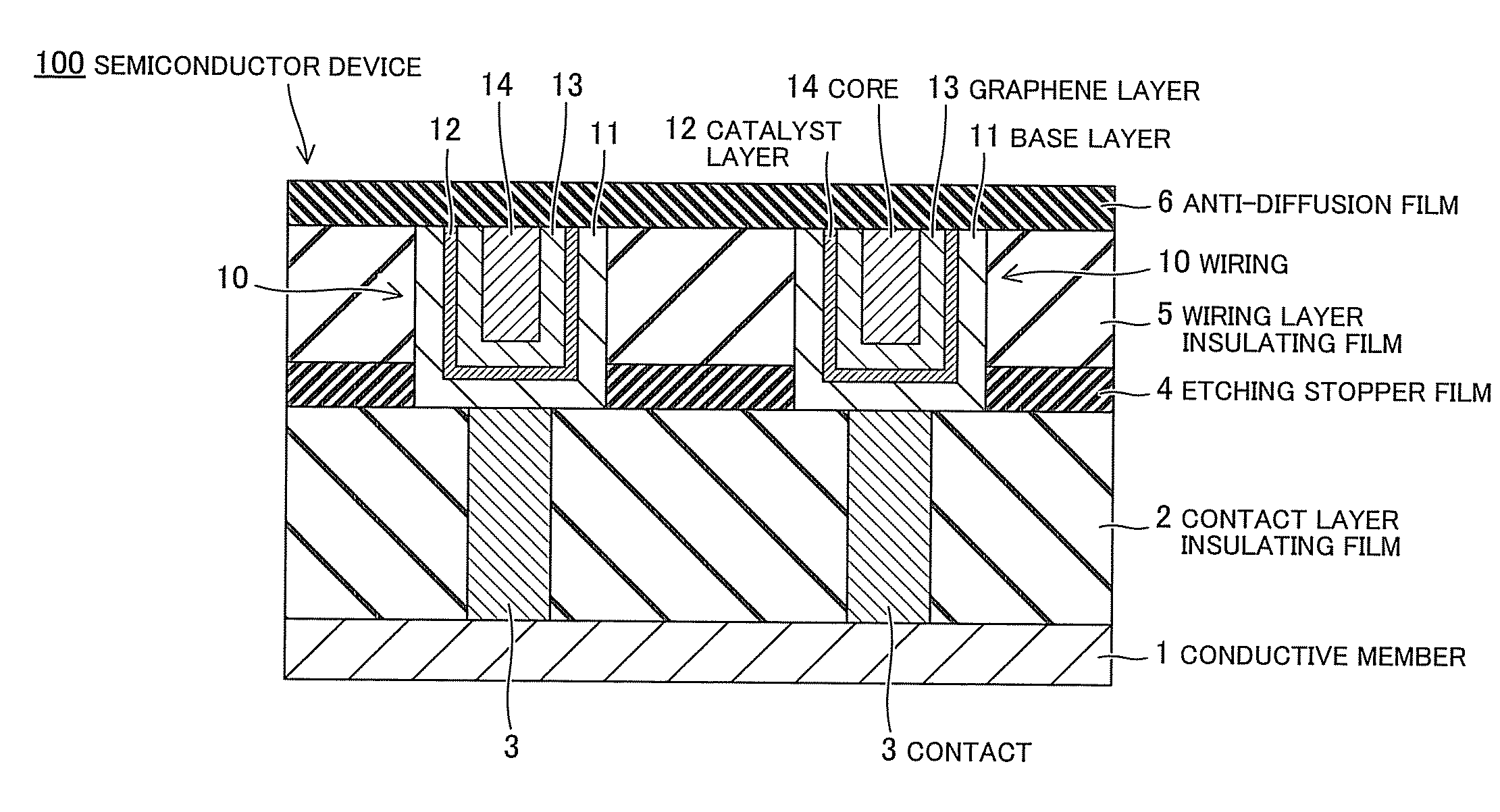
[0032]FIG. 1 is a cross sectional view of a semiconductor device 100 according to a first embodiment. The semiconductor device 100 has a wiring 10 formed in an etching stopper film 4 and a wiring layer insulating film 5 and having a single damascene structure, a contact 3 formed in a contact layer insulating film 2 for electrically connecting the wiring 10 as an upper layer and a conductive member 1 as a lower layer, and an anti-diffusion film 6 formed on the wiring 10 and the wiring layer insulating film 5.
[0033]The wiring 10 contains a core 14, a graphene layer 13 which is in contact with a bottom surface and both side surfaces of the core 14, a catalyst layer 12 which is in contact with a bottom surface and both side surfaces of the graphene layer 13, and a base layer 11 which is in contact with a bottom surface and both side surfaces of the catalyst layer 12.
[0034]The base layer 11 has a function of preventing diffusion of elements contained in the catalyst layer 12 into a perip...
second embodiment
[0070]The second embodiment is different from the first embodiment in that a contact is directly in contact with a graphene layer. Note that, the explanations will be omitted or simplified for the points same as the first embodiment.
[0071]FIGS. 5A and 5B are cross sectional views of a semiconductor device 200 according to a second embodiment. In addition, FIG. 6 is a top view of the semiconductor device 200. The cross sectional view taken on line A-A of FIG. 6 corresponds to FIG. 5A and the cross sectional view taken on line B-B corresponds to FIG. 5B. Note that, illustration of the wiring layer insulating film 5 and the anti-diffusion film 6 is omitted in FIG. 6.
[0072]The semiconductor device 200 has a wiring 20 formed in an etching stopper film 4 and a wiring layer insulating film 5 and having a damascene structure, a contact 25 formed in a contact layer insulating film 2 for electrically connecting the wiring 20 as an upper layer and a conductive member 1 as a lower layer, and an...
third embodiment
[0092]The third embodiment is different from the first embodiment in that a graphene layer is also formed on an upper surface of a core. Note that, the explanations will be omitted or simplified for the points same as the first embodiment.
[0093]FIG. 9 is a cross sectional view of a semiconductor device 300 according to a third embodiment.
[0094]The semiconductor device 300 has a wiring 30 formed in an etching stopper film 4 and a wiring layer insulating film 5 and having a single damascene structure, a contact 3 formed in a contact layer insulating film 2 for electrically connecting the wiring 30 as an upper layer and a conductive member 1 as a lower layer, and an anti-diffusion film 6 formed on the wiring 30 and the wiring layer insulating film 5.
[0095]The wiring 30 contains a core 34, a graphene layer 33a which is in contact with a bottom surface and both side surfaces of the core 34, a graphene layer 33b which is in contact with an upper surface of the core 34, a catalyst layer 12...
PUM
 Abstract
Description
Claims
Application Information