Gate line driving module for liquid crystal display and liquid crystal display using the same

a technology of liquid crystal display and driving module, which is applied in the direction of electric digital data processing, instruments, computing, etc., can solve the problems of easy generation of coupling between internal signals limitation of the gate line driver on the glass substrate in the amorphous silicon process, and increase of the internal parasitic capacitance of the gate line driver

Active Publication Date: 2011-01-13
INNOLUX CORP
View PDF5 Cites 2 Cited by
  • Summary
  • Abstract
  • Description
  • Claims
  • Application Information

AI Technical Summary

Benefits of technology

[0005]However, fabricating the gate line driver on the glass substrate in the amorphous silicon process has the limitation of which the gate line driver is simply implemented by N-type TFTs. As a result, a high level gate power source of the gate line driver must be supplied, such that the switch states of the internal switches are determined. However, the electron mobility of amorphous silicon is relatively low, width to length (W / L) ratios of the N-type TFTs adopted in the gate line driver must be relatively high to offset the low electron mobility of amorphous silicon. As a result, internal parasitic capacitance of the gate line driver is increased, such that the phenomenon of coupling between internal signals of the gate line driver is easily generated due to the increase of the parasitic capacitance. Accordingly, the output signals of the gate line driver creates a ripple effect, such that the display quality of the LC panel is affected. Furthermore, in the gate line driver, the N-type TFTs which are affected by bias over a long period of time have the phenomenon of device characteristic drift, so as to affect the operation of the gate line driver.

Problems solved by technology

However, fabricating the gate line driver on the glass substrate in the amorphous silicon process has the limitation of which the gate line driver is simply implemented by N-type TFTs.
As a result, internal parasitic capacitance of the gate line driver is increased, such that the phenomenon of coupling between internal signals of the gate line driver is easily generated due to the increase of the parasitic capacitance.
Accordingly, the output signals of the gate line driver creates a ripple effect, such that the display quality of the LC panel is affected.

Method used


Image

  • Gate line driving module for liquid crystal display and liquid crystal display using the same
  • Gate line driving module for liquid crystal display and liquid crystal display using the same
  • Gate line driving module for liquid crystal display and liquid crystal display using the same

Examples


Embodiment Construction

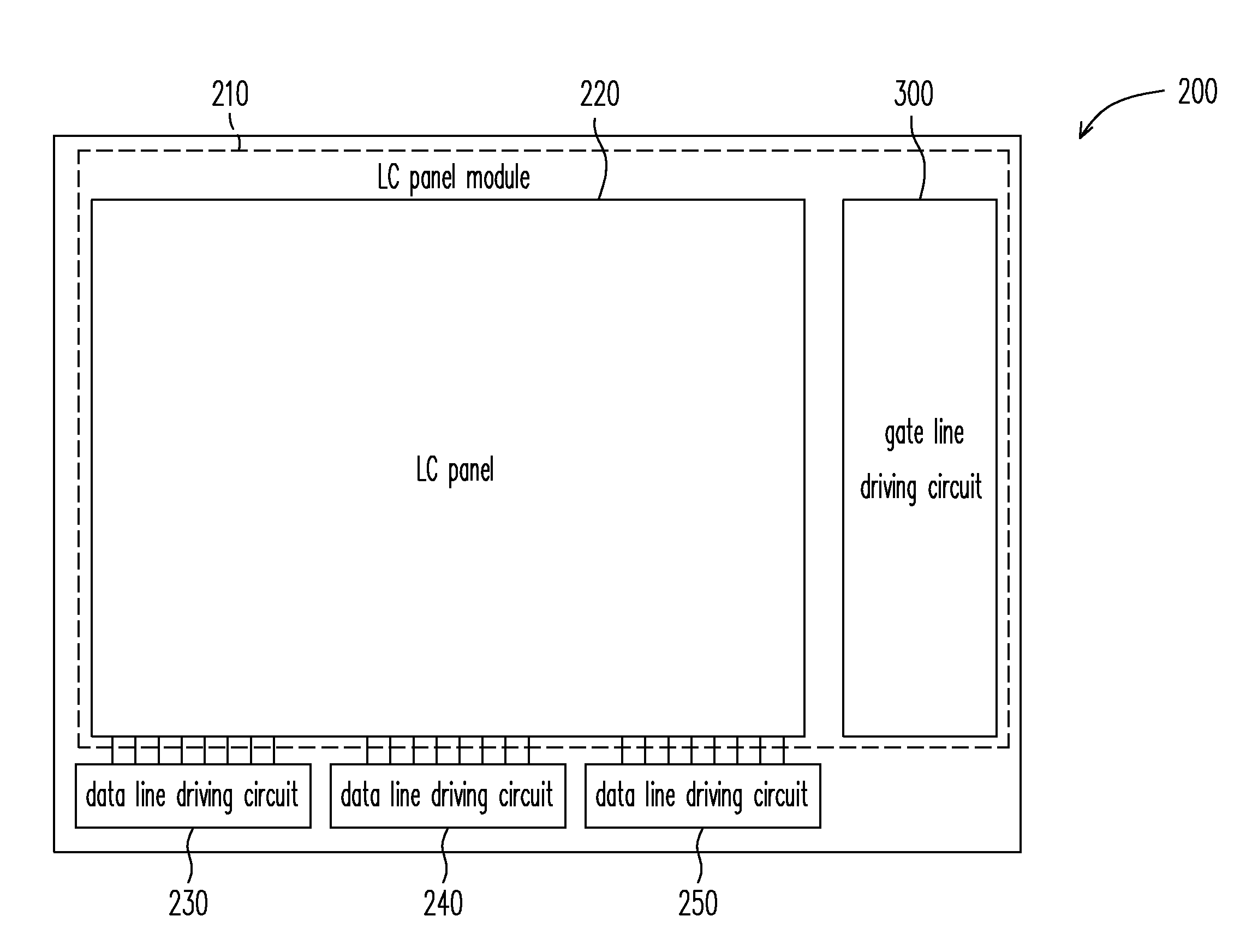
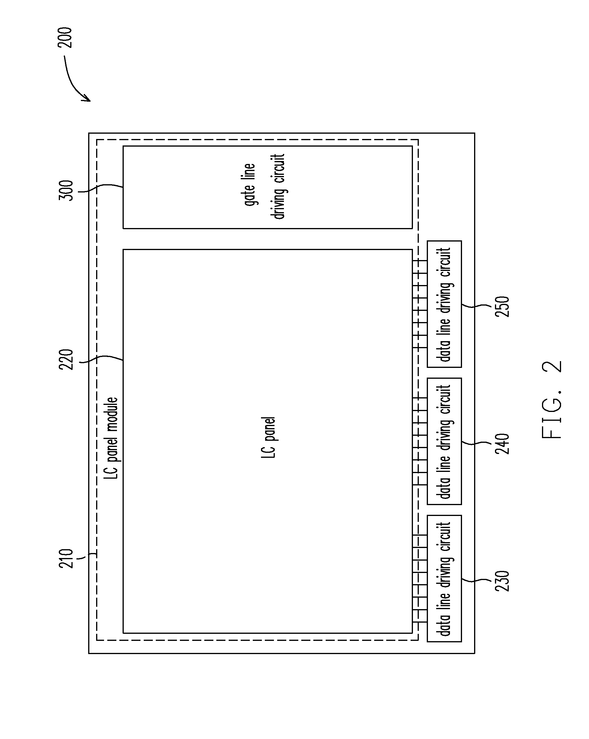
[0015]FIG. 2 is a schematic diagram of a TFT-LCD 200 using a gate line driving module 300 according to an embodiment of the disclosure. As shown in FIG. 2, the TFT-LCD 200 includes a liquid crystal (LC) panel module 210 and a plurality of data line driving circuits 230, 240, and 250. The LC panel module 210 includes an LC panel 220 and the gate line driving module 300. The LC panel 220 and the gate line driving module 300 are fabricated into the LC panel module 210 in an identical (or substantially similar) amorphous silicon process.

[0016]FIG. 3 is a schematic diagram of the gate line driving module 300 according to an embodiment of the disclosure. As shown in FIG. 3, the gate line driving module 300 has 240 gate line driving circuits including a 1st stage gate line driving circuit C_1, a 2nd stage gate line driving circuit C_2, a 3rd stage gate line driving circuit C_3, . . . , a 239th stage gate line driving circuit C_239, and a 240th stage gate line driving circuit C_240 and an a...


PUM


Abstract

A gate line driving module used on a liquid crystal display uses clock signal sources in replacement of a high level gate power source, such that the phenomenon of device characteristic drift occurring in the foregoing related art is avoided. The gate line driving module includes a plurality of odd-pixel gate line driving circuits, a plurality of even-pixel gate line driving circuits, and an auxiliary gate line driving circuit. A pair of neighboring odd-pixel gate line driving circuit and even-pixel gate line driving circuit exchange output signals thereof with each other in a forward or feedback manner for ensuring that each the odd-pixel gate line driving circuit and each the even-pixel gate line driving circuit are driven once. The auxiliary gate line driving circuit is used for ensuring that signal iteration of the gate line driving module is under normal operation.

Description

BACKGROUND OF THE DISCLOSURE[0001]1. Field of the Disclosure[0002]The disclosure relates to a gate line driving module for a liquid crystal display (LCD), and more particularly, the disclosure relates to a gate line driving module and an LCD which use clock signals to serve as a high level gate power source.[0003]2. Description of Related Art[0004]FIG. 1 is a schematic view of a typical thin film transistor liquid crystal display (TFT-LCD) 100. As shown in FIG. 1, the TFT-LCD 100 includes a liquid crystal (LC) panel 110, a gate line driver 120, and a plurality of data line drivers 130, 140, and 150. The gate line driver 120 and the data line drivers 130, 140, and 150 drive corresponding thin film transistors (TFTs) on the LC panel 110. In order to reduce the cost of manufacturing TFT-LCDs, it is currently considered that the gate line driver and the LC panel are fabricated on the glass substrate in an identical process. By such a manner, the cost of additionally disposing the gate l...

Claims


Application Information

Patent Timeline
Patent Type & Authority Applications(United States)
IPC IPC(8): G06F3/038
CPCG02F1/13454G02F2202/103G09G3/3674G09G2300/0408G09G2320/043G09G3/3266G09G2330/06G09G3/3677G09G2310/0278G09G2310/0286G09G2330/02
Inventor CHIANG, CHIEN-HSUEHCHEN, SZ-HSIAO
Owner INNOLUX CORP
Why Eureka
Try Eureka