Display panel driving circuit, liquid crystal device, shift register, liquid crystal panel, and driving method of display device

a technology of display panel and driving circuit, which is applied in the direction of digital storage, instruments, computing, etc., can solve the problems of disordered clock signal, small pulse width of gate on-pulse signal, so as to reduce circuit area, prevent display disorder, and increase load

Active Publication Date: 2011-01-27
SHARP KK
View PDF24 Cites 29 Cited by
  • Summary
  • Abstract
  • Description
  • Claims
  • Application Information

AI Technical Summary

Benefits of technology

[0057]According to the display panel driving circuit of the present invention, once a clear signal is made active due to anomalousness in a sync signal, pulse output from the shift register stops thereafter. Therefore, it is possible to prevent disorder of display and hold down an increase in load given to the power source.
[0058]Moreover, accordin

Problems solved by technology

Moreover, for example if a noise generates in the horizontal sync signal HSYNC, the clock signal becomes disordered, and anomalousness that a pulse width of the gate on-pulse signal becomes small may continue until

Method used


Image

  • Display panel driving circuit, liquid crystal device, shift register, liquid crystal panel, and driving method of display device
  • Display panel driving circuit, liquid crystal device, shift register, liquid crystal panel, and driving method of display device
  • Display panel driving circuit, liquid crystal device, shift register, liquid crystal panel, and driving method of display device

Examples


embodiment 1

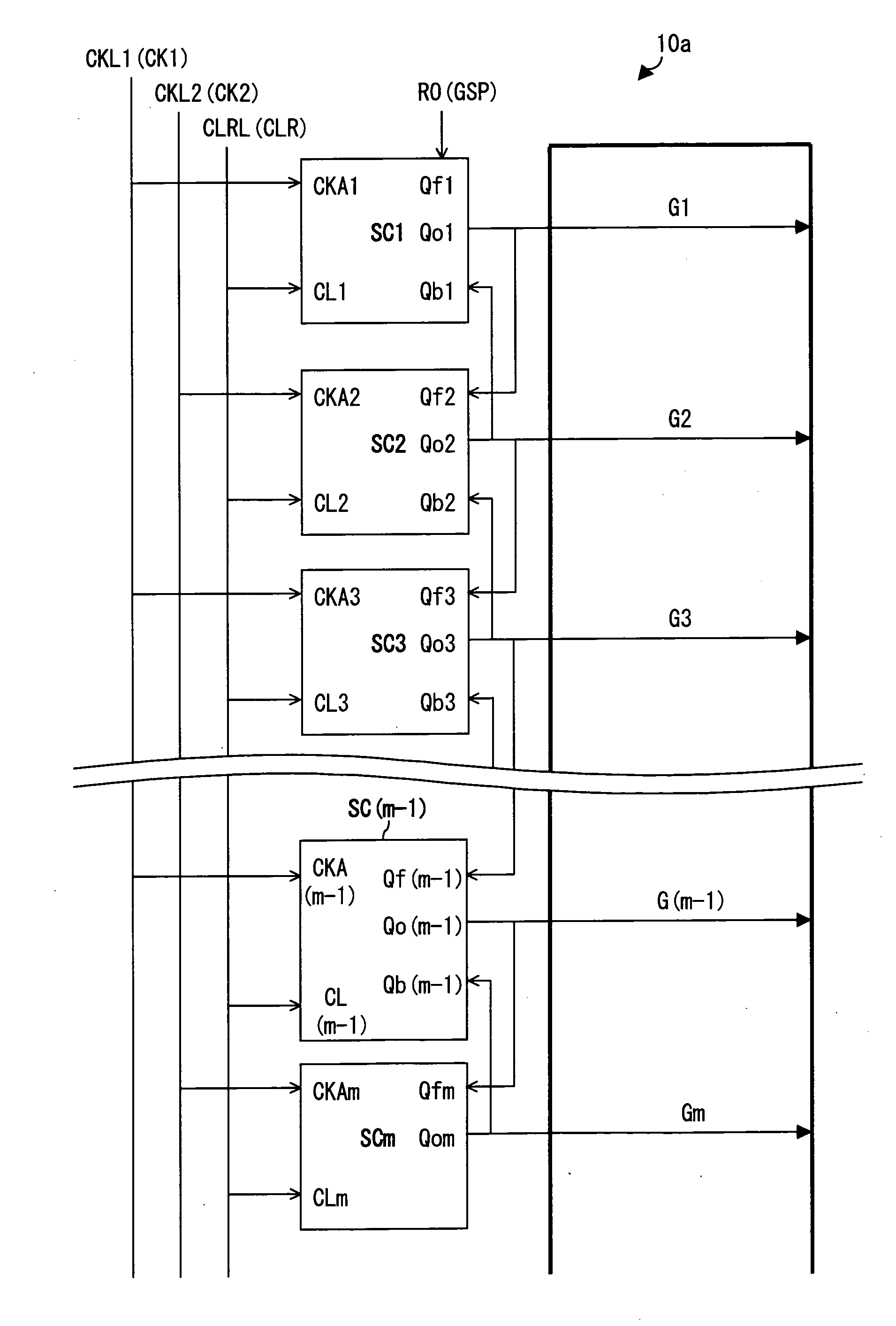
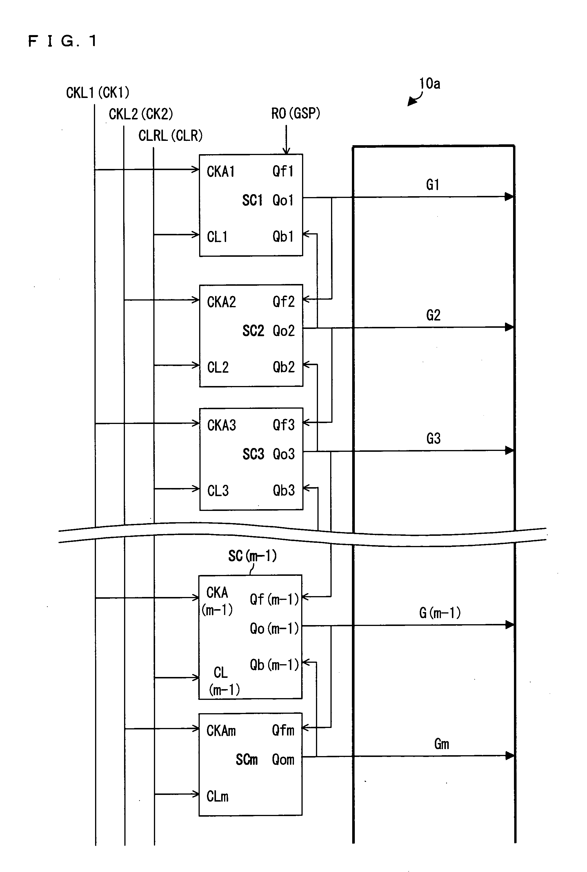
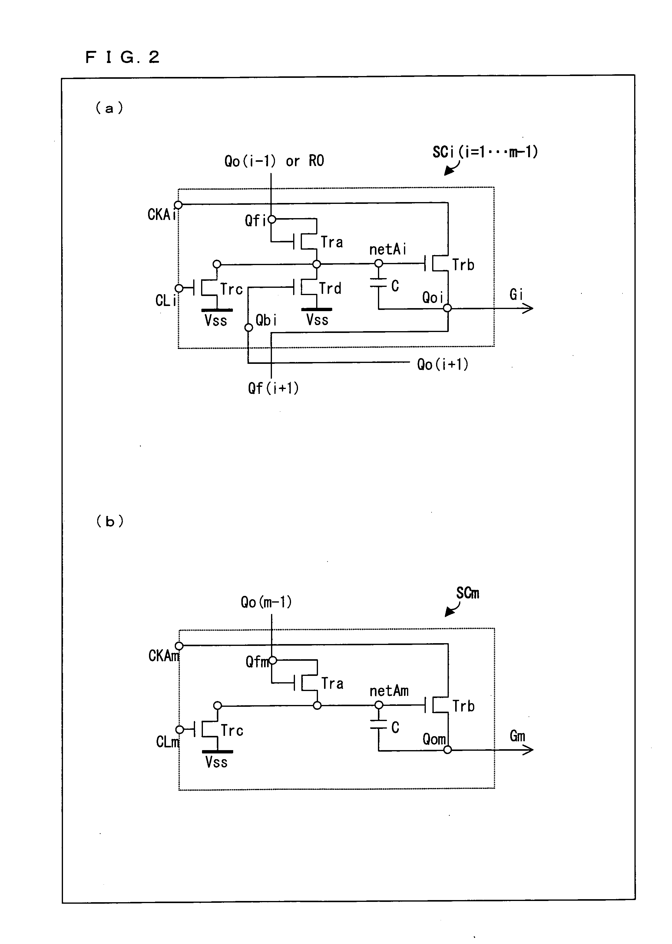
[0123]FIG. 1 illustrates a configuration of a shift register 10a in accordance with the present Embodiment 1. As shown in FIG. 1, the shift register 10a is made up of a plurality of shift circuits (unit circuits) SC1, SC2, . . . and SCm connected in stages. Each of the shift circuits SCi (i=1, 2, 3, . . . and m−1) includes input nodes Qfi, Qbi, CKAi, and CLi, and an output node Qoi. The shift circuit SCm includes input nodes Qfm, CKAm, and CLm, and an output node Qom.

[0124]The shift circuit SC1 has its node Qf1 be connected to a GSP output terminal RO of the level shifter (see FIG. 23). Further, the shift circuit has its node Qb1 be connected to the node Qo2 of a shift circuit SC2, has its node CKA1 be connected to a first clock line CKL1 to which a first clock signal is supplied, and has its node CL1 be connected to a clear line CLRL to which a clear signal (CLR) is supplied. Further, the shift circuit SC1 outputs a gate on-pulse signal (signal line selection signal) G1 via its nod...

embodiment 2

[0181]FIG. 19 illustrates a configuration of a liquid crystal panel of the present Embodiment 2. According to the liquid crystal panel illustrated in FIG. 19, a shift register 10f is provided on a left end of the liquid crystal panel, and a shift register 10g is provided on a right end of the liquid crystal panel. The shift register 10f is made up of a plurality of shift circuits SCi (i=1, 3, 5, . . . and 2n+1) connected in stages, and a plurality of shift circuits SCi (i=2, 4, 6, . . . and 2n) connected in stages. Each of the shift circuits SCi (i=1, 2, 3, . . . and 2n−2) includes input nodes Qfi, Qbi, CKAi, CKBi, and CLi, and an output node Qoi. A shift circuit SC(2n−1) includes input nodes Qf(2n−1), CKA(2n−1), CKB(2n−1), and CL(2n−1), and an output node Qo(2n−1). Moreover, a shift circuit SC(2n) includes input nodes Qf(2n), CKA(2n), CKB(2n), and CL(2n), and an output node Qo(2n).

[0182]The shift circuit SC1 has its node Qf1 be connected to a GSP1 output terminal RO1 of a level shi...

embodiment 3

[0213]Embodiment 3 is as described below, with reference to FIGS. 24 to 36.

[0214]FIG. 24 is a block diagram illustrating a configuration of the present liquid crystal display device. As illustrated in FIG. 24, the present liquid crystal display device 101 includes a liquid crystal panel 103, a gate driver 105, a source driver 106, a timing controller 107, and a data processing circuit 108. The gate driver 105 includes a shift register 110 and a level shifter 104, and the gate driver 105 and the timing controller 107 construct a liquid crystal panel driving circuit 111. In the present embodiment, the level shifter 104 is included in the gate driver 105; however, the level shifter 104 may be provided outside of the gate driver 105.

[0215]The present liquid crystal panel 103 includes scanning signal lines 16 that are driven by the gate driver 105, data signal lines 15 that are driven by the source driver 106, pixels P, retention capacitor wires (not illustrated) and the like, and the sh...


PUM


Abstract

A display panel drive circuit includes a shift register constructed of unit circuits connected in stages. The unit circuits generate signal line selection signals, respectively, which signal line selection signals are made active for a respective certain period of time to form a respective pulse, and the pulses are outputted successively from respective unit circuits in order of ordinal number starting from a first stage until an end stage. In at least one embodiment, each of the unit circuits receive (i) clock signals generated based on a sync signal received from outside of the display panel drive circuit, (ii) a start pulse signal generated based on the sync signal, or a signal line selection signal generated in a stage different from its own stage, and (iii) a clear signal. The clear signal is made active in a case where anomalousness is included in the sync signal, and no pulse is outputted from the shift register until a subsequent vertical scanning period starts. This configuration achieves a display panel drive circuit which prevents display disorder or holds down increase in load given to a power source, each of which occurs in a case where anomalousness is included in the sync signal.

Description

TECHNICAL FIELD[0001]The present invention relates to a display panel driving circuit and a shift register for use in such a display panel driving circuit.BACKGROUND ART[0002]FIG. 40 is a circuit diagram illustrating a conventional shift register for use in a gate driver that is included in a liquid crystal display device. As shown in FIG. 40, a conventional shift register 100 is made up of a plurality of shift circuits (unit circuits) sc1, sc2, . . . scm, and scd, which are connected in stages. Each of the shift circuits sci (i=1, 2, 3, . . . or m) includes input nodes qfi, qbi, and CKAi, and an output node qoi. The shift circuit scd, which is a dummy shift circuit, includes input nodes qfd and CKAd and an output node qod.[0003]The shift circuit sc1 has its node qf1 be connected to an output terminal via which a gate start pulse signal GSP is outputted, has its node qb1 be connected to the node qo2 of the shift circuit sc2, and has its node CKA1 be connected to a first clock line C...

Claims


Application Information

Patent Timeline
IPC IPC(8): G09G5/00
CPCG09G3/3677G09G2310/0286G11C19/28G11C19/184G09G2330/025
Inventor MIZUNAGA, TAKAYUKIMORII, HIDEKIIWAMOTO, AKIHISAHIROKANE, MASAHIROOHTA, YUUKI
Owner SHARP KK
Why Eureka
Try Eureka