Generating integrated circuit floorplan layouts

a technology for integrated circuits and floorplans, applied in the field of computer-aided design tools for generating integrated circuit floorplan layouts, can solve the problems of users not performing a floorplan analysis early, the prior-art floor-planning tools cannot work for pure register transfer level (rtl) descriptions, and the process can be relatively time-consuming and cumbersom

Inactive Publication Date: 2011-01-27
BELL SEMICON LLC
View PDF24 Cites 15 Cited by
  • Summary
  • Abstract
  • Description
  • Claims
  • Application Information

AI Technical Summary

Benefits of technology

[0007]Disclosed herein are various embodiments of a method of generating a floorplan layout of an integrated circuit (IC) that is amenable to implementation in a computer-aided design (CAD) tool. The method is capable of performing placement and routing processing for the IC while requiring very little information about the specific circuitry used in various functional blocks of the IC. For example, at the time of the placement and routing processing, one or more functional blocks of the IC can be

Problems solved by technology

With the CAD tools that are currently available on the market, this process can be relatively time consuming and cumbersome because it involves many manual tasks.
For example, during early design phases, when gate-level netlists are not yet reasonably complete, a layout engineer might be fo

Method used


Image

  • Generating integrated circuit floorplan layouts
  • Generating integrated circuit floorplan layouts
  • Generating integrated circuit floorplan layouts

Examples


Embodiment Construction

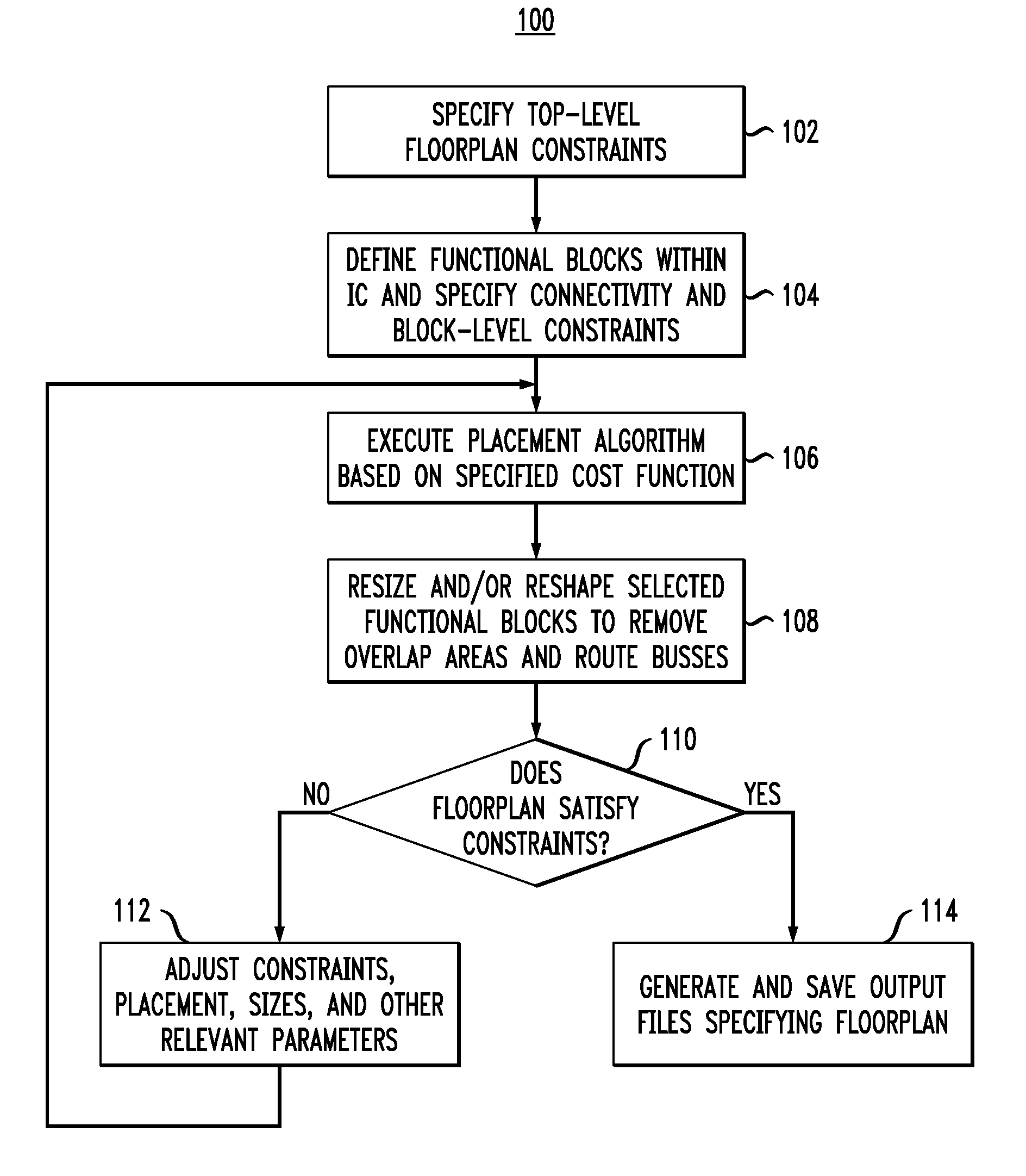
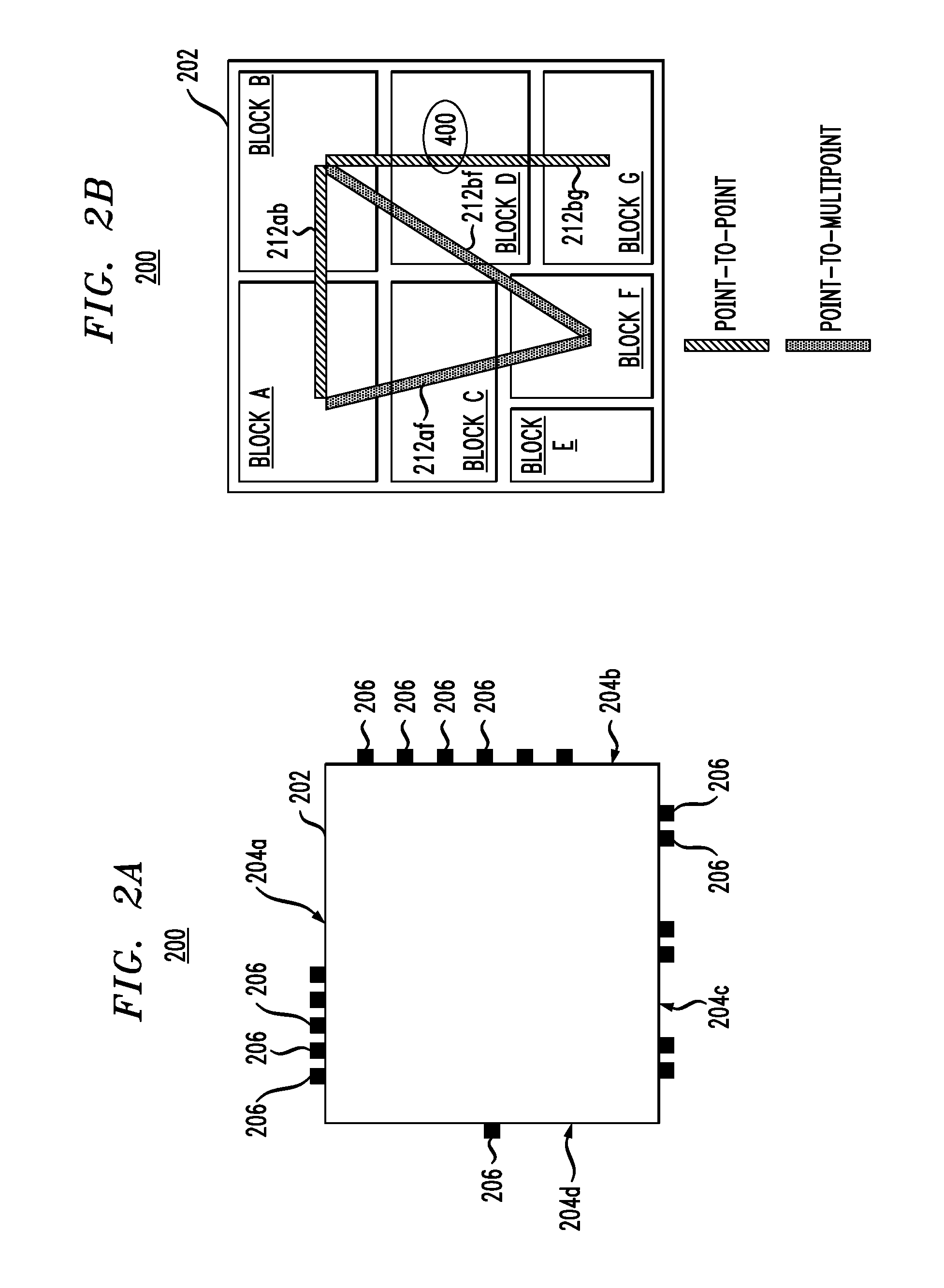
[0015]FIGS. 1 and 2A-E illustrate a method 100 of generating IC layouts according to one embodiment of the invention. More specifically, FIG. 1 shows a flowchart of method 100. FIGS. 2A-E show representative IC layouts corresponding to different steps of method 100. In general, method 100 is amenable to being implemented as part of a software package or suite for computer-aided design (CAD) of ICs.

[0016]Referring to FIG. 1, at step 102 of method 100, top-level floorplan constraints are specified. Top-level floorplan constraints may include, but are not limited to, (i) an upper limit on the area occupied by the IC; (ii) an aspect ratio of a boundary box corresponding to the IC; and (iii) pin locations on the perimeter of the IC. The top-level floorplan constraints can be specified by the user through a CAD interface or read from a corresponding input file.

[0017]FIG. 2A schematically shows an example of the top-level floorplan constraints corresponding to step 102. More specifically, ...


PUM


Abstract

A method of generating a floorplan layout of an integrated circuit (IC) that is amenable to implementation in a computer-aided design tool. The method is capable of performing placement and routing processing for the IC while requiring very little information about the specific circuitry used in various functional blocks of the IC. For example, at the time of the placement and routing processing, one or more functional blocks of the IC can be specified as empty functional blocks and/or functional blocks that are only partially rendered in gates.

Description

BACKGROUND[0001]1. Field of the Invention[0002]The present invention relates generally to the design and fabrication of integrated circuits (ICs) and, more specifically but not exclusively, to computer-aided design (CAD) tools for generating IC layouts.[0003]2. Description of the Related Art[0004]This section introduces aspects that may help facilitate a better understanding of the invention(s). Accordingly, the statements of this section are to be read in this light and are not to be understood as admissions about what is in the prior art or what is not in the prior art.[0005]An IC layout is a representation of an integrated circuit in terms of planar geometric shapes corresponding to various sub-circuits, such as functional blocks, interfaces, and / or individual circuit elements. Since the behavior and performance of an IC depends on the positions of and interconnections between its sub-circuits, a layout engineer aims to place and connect the sub-circuits on a chip so that certain...

Claims


Application Information

Patent Timeline
IPC IPC(8): G06F17/50
CPCG06F17/5072G06F30/392
Inventor DIRKS, JUERGENMUELLER, NORBERTBLOCK, STEFAN
Owner BELL SEMICON LLC
Why Eureka
Try Eureka