Manufacturing method for molding image sensor package structure and image sensor package structure thereof

a manufacturing method and image sensor technology, applied in semiconductor/solid-state device manufacturing, semiconductor devices, electrical devices, etc., can solve the problems of high cost, time-consuming dispensing, and high cost of traditional image sensor package technology, and achieve the effect of reducing the cost of mold preparation, extending the blockage to invasive moisture, and improving the reliability of image sensor package structur

Active Publication Date: 2011-02-03
TONG HSING ELECTRONICS INDS
View PDF5 Cites 45 Cited by
  • Summary
  • Abstract
  • Description
  • Claims
  • Application Information

AI Technical Summary

Benefits of technology

[0018]2. By virtue of the dam arranged on the transparent lid, there is no need to make the mold with a custom-made inward-extending section for varying lid dimensions, which significantly reduces costs for preparing the mold.
[0019]3. The dam on the transparent lid allows the mold compound to cover around the chip, the transparent lid, and the dam, thereby extending the blockage to invasive moisture.
[0020]4. The existence of the dam allows the mold to depress against the top of the dam and allows the mold compound protect the periphery of the transparent lid to prevent moisture from invading the air cavity underneath the transparent lid, thereby improving the reliability of the image sensor package structure.
[0021]5. The image sensor package structure is produced by means of molding so as to significantly shorten processing cycle time and increase throughput.
[0022]6. The molding formation and batch-type production of the image sensor package structure facilitate the reduction of the processing costs of the image sensor package structure.
[0023]7. The disadvantages of the known technology related to the costly liquid compound and the time-consuming dispensing process are eliminated.

Problems solved by technology

However, the macromolecular liquid compound is quite costly and needs to be arranged through a time-consuming dispensing process.
Consequently, the traditional technology of such image sensor package is disadvantageous in its prolonged processing cycle and high cost.
However, the inward-extending section could significantly increase the cost for making the upper mould half, and is unfavorable to the purpose of reducing the overall cost of the image sensor package.
Even when the elastic material is used, the known method for encapsulating a chip still puts the image sensor in risk from damage, thus leading to a decreased yield rate.

Method used


Image

  • Manufacturing method for molding image sensor package structure and image sensor package structure thereof
  • Manufacturing method for molding image sensor package structure and image sensor package structure thereof
  • Manufacturing method for molding image sensor package structure and image sensor package structure thereof

Examples


Embodiment Construction

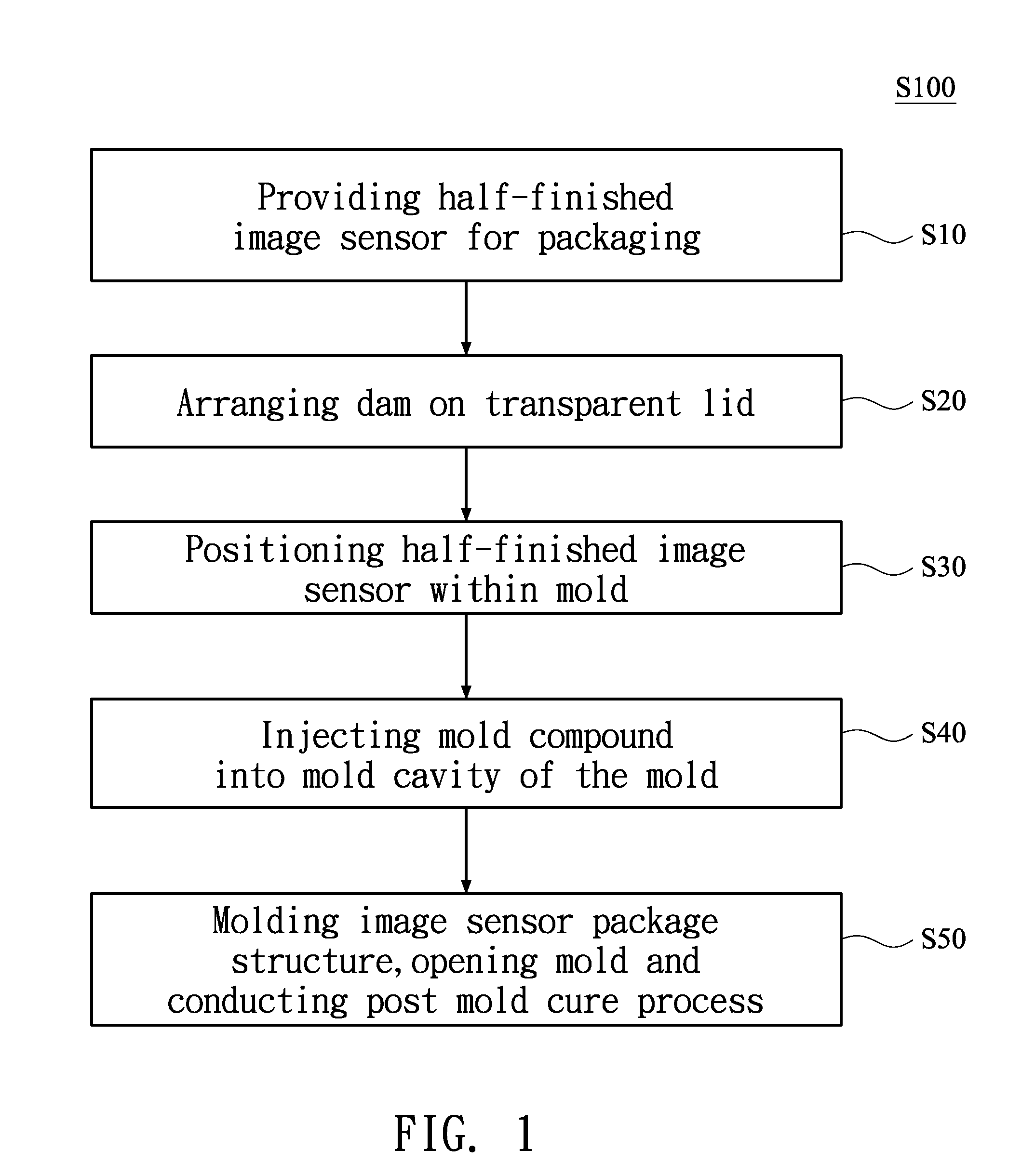
[0039]Referring to FIG. 1, the present embodiment is a method (S100) for molding an image sensor package structure. The method (S100) includes the following steps: providing a half-finished image sensor for packaging (S10); arranging a dam on a transparent lid (S20); positioning the half-finished image sensor within a mold (S30); injecting a mold compound into the mold cavity of the mold (S40); and molding the image sensor package structure, opening the mold and conducting a post mold cure process (S50).

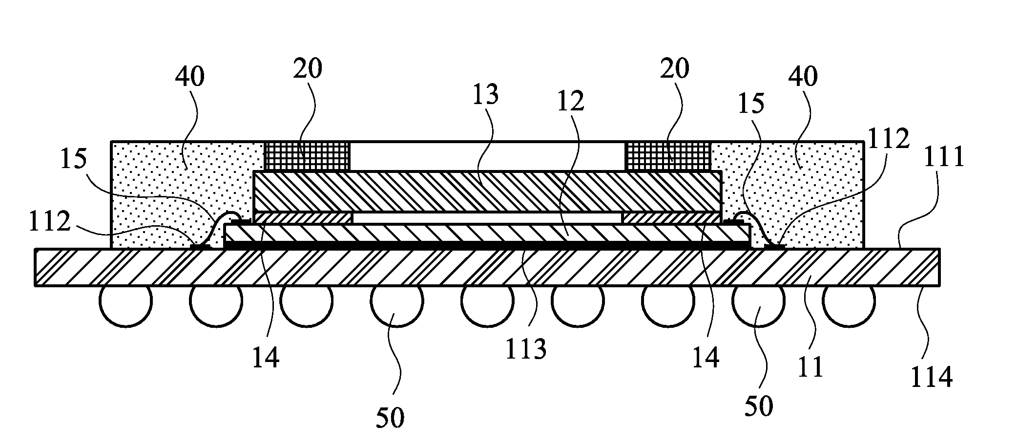
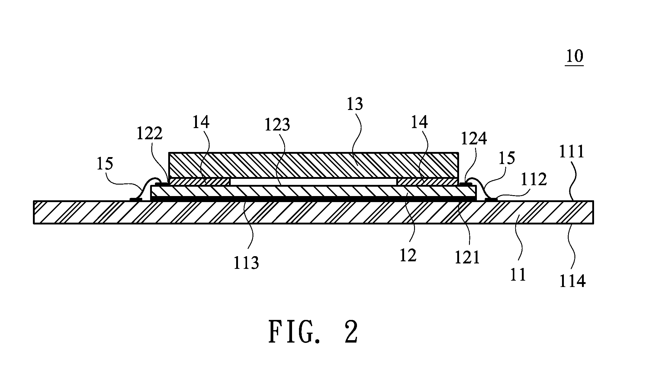
[0040]In the step of providing a half-finished image sensor for packaging (S10), as shown in FIG. 2, a half-finished image sensor 10 for packaging is provided. The half-finished image sensor 10 has a substrate 11, at least one chip 12, and at least one transparent lid 13. Alternatively, as shown in 5A, multiple said chips 12 are provided on the same substrate 11 for producing multiple said image sensor package structures simultaneously.

[0041]The substrate 11 may be one conventionally...


PUM


Abstract

A manufacturing method for molding an image sensor package structure and the image sensor package structure thereof are disclosed. The manufacturing method includes following steps of providing a half-finished image sensor for packaging, arranging a dam on the peripheral of a transparent lid of the half-finished image sensor, positioning the half-finished image sensor within a mold, and injecting a mold compound into the mold cavity of the mold. The dam is arranged on the top surface of the transparent lid and the inner surface of the mold can exactly contact with the top surface of dam so that the mold compound injected into the mold cavity is prevented from overflowing to the transparent lid by the dam. Furthermore, the arrangement of the dam and the mold compound can increase packaged areas and extend blockage to invasive moisture so as to enhance the reliability of the image sensor package structure.

Description

BACKGROUND OF THE INVENTION[0001]1. Technical Field[0002]The present invention relates to semiconductor packaging structures. More particularly, the present invention relates to a manufacturing method for molding image sensor package structure and an image sensor package structure made through the method.[0003]2. Description of Related Art[0004]Conventionally, an image sensor package is made by placing an image sensor chip on a substrate, connecting the image sensor chip and the substrate by means of metal conducting wires, and mounting a transparent lid (e.g. glass) upon the image sensor chip so as to allow light to pass through the transparent lid and get acquired by the sensor chip. The resultant image sensor package is for a system manufacturer to integrate to an external device, such as a printed circuit board, or to apply to any of various electronic products such as a DSC (Digital Still Camera), a DV (Digital Video), a security monitoring system, a mobile phone, or a vehicle ...

Claims


Application Information

Patent Timeline
Patent Type & Authority Applications(United States)
IPC IPC(8): H01L31/02H01L31/18
CPCH01L27/14618H01L31/0203H01L2924/1815H01L2224/97H01L2924/15311H01L2224/73265H01L2224/48227H01L24/97H01L2224/32225H01L2224/48091H01L2924/00014H01L2924/00H01L2924/181
Inventor TU, HSIU-WENKUO, REN-LONGSHIAO, YOUNG-HOUNGCHEN, TSAO-PINHO, MON-NAMHSU, CHIH-CHENGLIN, CHIN-FUHSIN, CHUNG-HSIEN
Owner TONG HSING ELECTRONICS INDS
Why Eureka
Try Eureka