Organic el device

Inactive Publication Date: 2011-02-03
ROHM CO LTD
View PDF3 Cites 7 Cited by
  • Summary
  • Abstract
  • Description
  • Claims
  • Application Information

AI Technical Summary

Benefits of technology

[0021]According to the present invention, the first connecting surface of the first external terminal connected to the first electrode of surface shape is formed more largely than the second connecting surface of the second external terminal connected to the second electrode having small electric resistance. Accordingly, in the present invention, since the carrier implanted into the first electrode can be increased, the carrier which reaches the center of the organic light emitting layer via the first electrode can be increased. As a result, in the present invention, since the light emitted in the center of the organic light emitting layer can be increased, the mottle of luminance distribution can be reduced.
[0022]Moreover, according to the present invention, the electric charge of the hole, the electron, etc. can be fed into the desire region of the first electrode by the convex connecting member and the conductive feed unit member. Accordingly, the electric charge can be implanted also into the region to which it is hard to feed the electric charge, such as the central part of the organic light emitting layer. As a result, the mottle of the luminance distribution of the light emitted in the organic light emitting layer can be reduced.
[0023]Furthermore, according to the present invention, the feed unit member is disposed to the opposite side of the first electrode sandwiching the organic light emitting layer. Accordingly, since the light irradiated to the external is not shielded after the light which transmits the first electrode by the feed unit member, the extraction of the light emitted by the organic light emitting layer can be improved.

Problems solved by technology

In such the case, there was a problem that a mottle of a luminance distribution occurred within a surface of a light emitting surface in an organic EL device.

Method used


Image

  • Organic el device
  • Organic el device
  • Organic el device

Examples


first embodiment

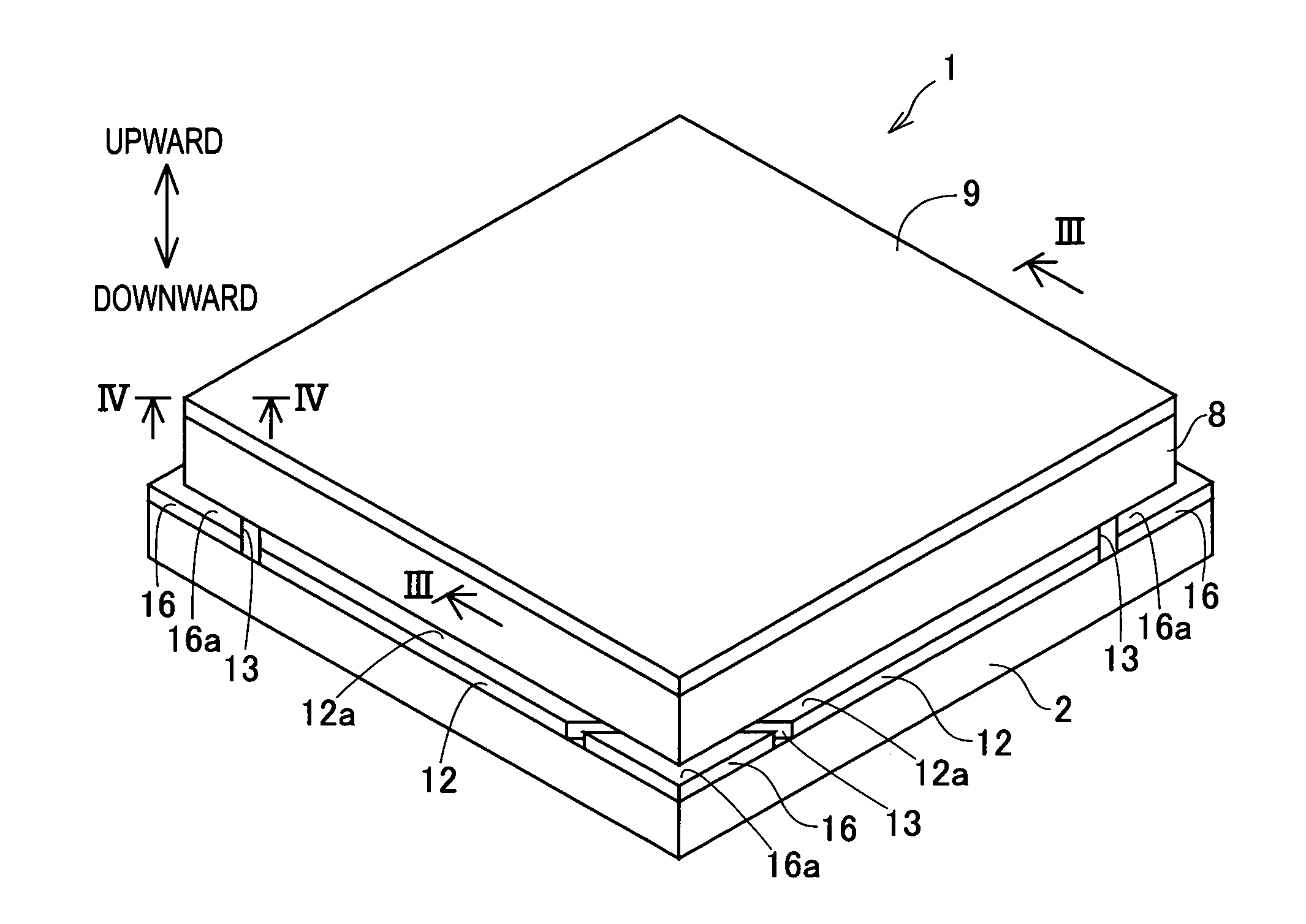
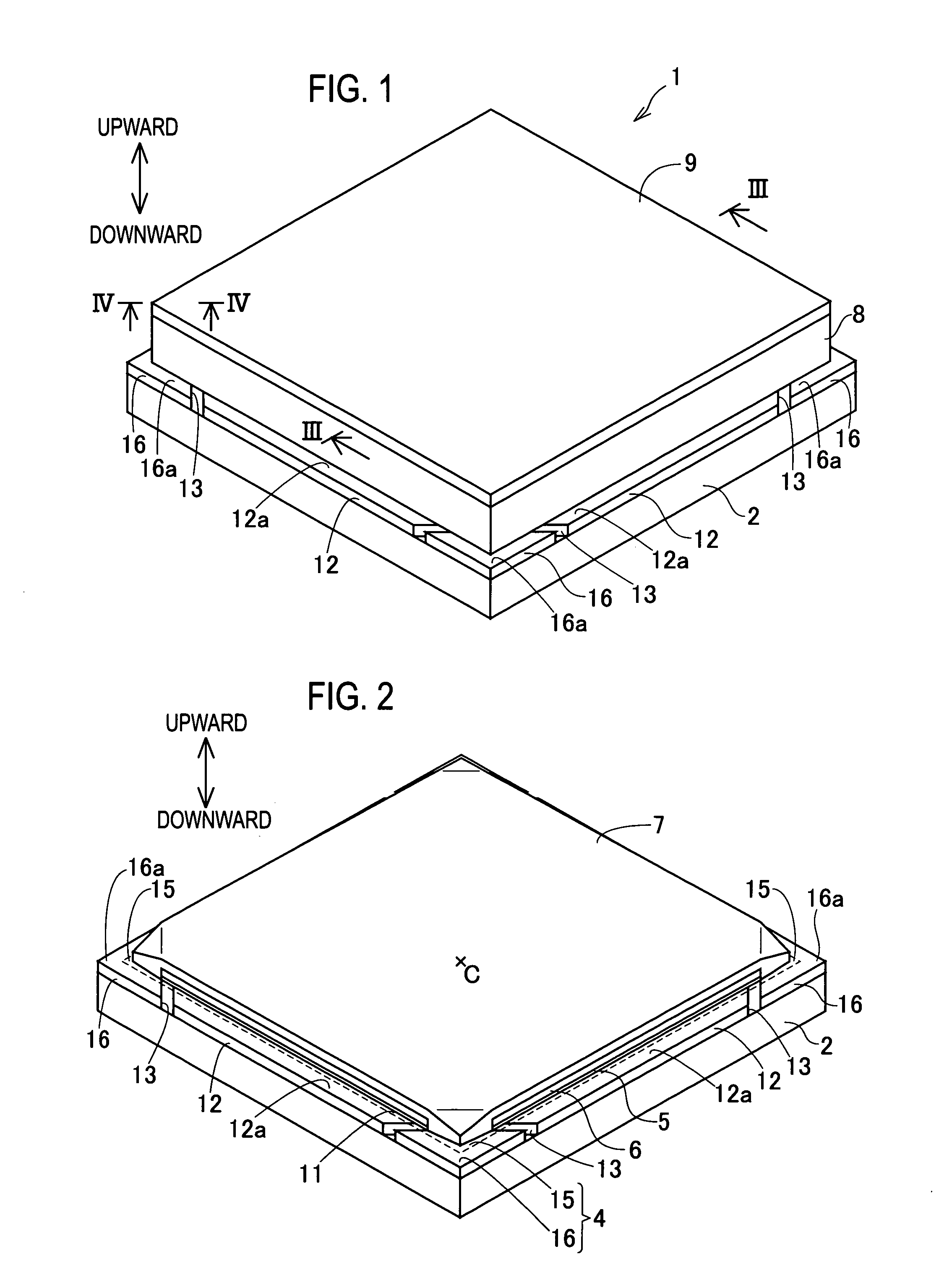
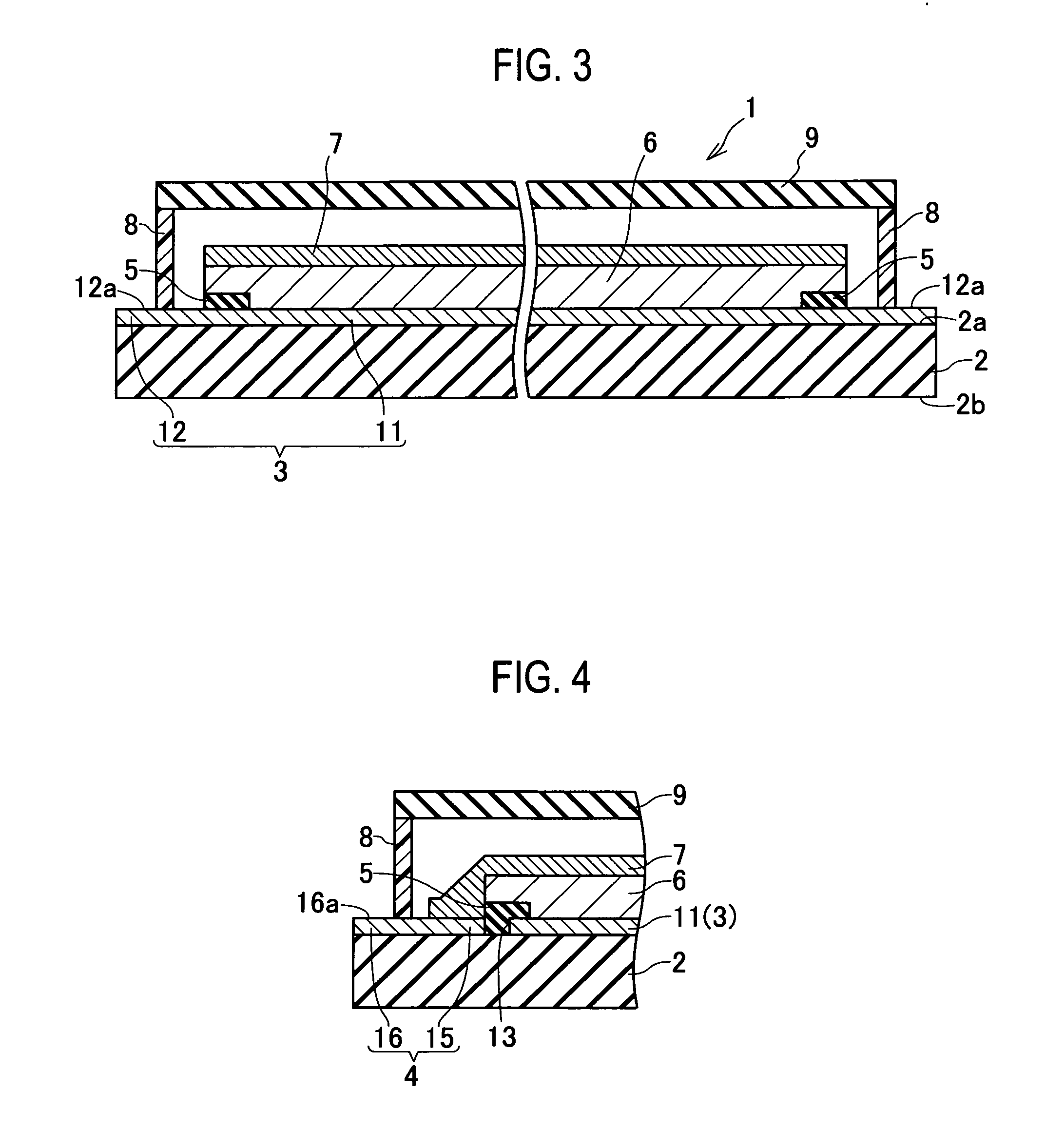
[0063]Hereinafter, a first embodiment that applied the present invention to a bottom emission type organic EL device will be described, with reference to drawings. FIG. 1 is a whole perspective diagram showing an organic EL device according to the first embodiment. FIG. 2 is a whole inside perspective diagram showing the organic EL device which removed a sealing plate. FIG. 3 is a cross-sectional diagram taken in line of FIG. 1. FIG. 4 is a cross-sectional diagram taken in line IV-IV of FIG. 1. FIG. 5 is a top view showing a first transmissible electrode and a second transmissible electrode. In the following explanation, upward and downward shown by an arrow of FIG. 1 is applied to an up-and-down direction.

[0064]As shown in FIG. 1 to FIG. 5, the organic EL device 1 according to the first embodiment includes: a substrate 2; a first transmissible electrode 3; a second four transmissible electrodes 4; an insulating layer 5; an organic light emitting layer 6; a cathode (second electrode...

second embodiment

[0097]Next, an organic EL device according to a second embodiment that modified a part of the first embodiment mentioned above will be explained, with reference to drawings. FIG. 16 is a whole perspective diagram showing the organic EL device accroding to the second embodiment. FIG. 17 is a top view showing a transmissible electrode. In FIG. 16, dashed lines show a sealing material 8 and a sealing plate 9 for convenience. Also, in FIG. 17, dashed lines show the periphery of the sealing material 8. The same configuration as the first embodiment attaches the same reference numeral, and therefore omits the explanation.

[0098]As shown in FIG. 16 and FIG. 17, in the organic EL device 1A according to the second embodiment, the shape of the first transmissible electrode 3A and the second transmissible electrode formed on the substrate 24A is different from that of the first embodiment.

[0099]The first transmissible electrode 3A is formed in the cross shape in regions except near the vertex o...

third embodiment

[0102]Next, an organic EL device according to a third embodiment that modified a part of the first embodiment mentioned above will be explained, with reference to drawings. FIG. 18 is a top view of a transmissible electrode according to the third embodiment. In FIG. 18, dashed lines show the periphery of the sealing material 8. In addition, the same configuration as the embodiment mentioned above attaches the same reference numeral, and therefore omits the explanation.

[0103]As shown in FIG. 18, in the organic EL device according to the third embodiment, the shapes of the first transmissible electrode 3B formed on the growth principal surface 2a of the substrate 2 (refer to FIG. 3) and the second transmissible electrodes 4B are different from the first embodiment.

[0104]The first transmissible electrode 3B is formed in the approximately whole surface of the growth principal surface 2a except that the central part of each side of the growth principal surface 2a of the substrate 2 is re...


PUM


Abstract

The organic EL device (1) comprises: a substrate (2); a light emitting unit formed on the substrate (2), and including an anode (11), a cathode (7) having anelectric resistance lower than that of the anode (11), an organic light emitting layer (6) formed between the anode (11) and the cathode (7); an anode terminal (12) formed on the substrate (2) and connected to the anode (11), and a cathode terminal (16) formed on the substrate (2) and connected to the cathode (7). A surface of the anode terminal (12) connected to the external is applied into an anode connecting surface (12a), and a surface of the cathode terminal (16) connected to the external is applied into a cathode connecting face (16a). The size (S1) of the anode connecting surface (12a) is larger than the size (S2) of the cathode connecting surface (16a).

Description

TECHNICAL FIELD[0001]The present invention relates to an organic electroluminescence (EL) device having an organic light emitting layer inserted into a pair of electrodes from which electric resistance is different.[0002]Also, the present invention relates to an organic EL device having a light transmissible electrode.BACKGROUND ART[0003]An organic EL device having an organic light emitting layer is known conventional. Moreover, in order to use for lighting etc., it is in the tendency that a plane area of an organic EL device enlarges. In such the case, there was a problem that a mottle of a luminance distribution occurred within a surface of a light emitting surface in an organic EL device. Accordingly, it is proposed the technology for reducing the mottle of the luminance distribution of such the organic EL device.[0004]Patent Literature 1 discloses an organic EL lighting device having a substrate, an anode formed on the substrate, an organic light emitting layer, and a cathode. I...

Claims


Application Information

Patent Timeline
IPC IPC(8): H01L51/52
CPCH01L51/5203H10K50/805
Inventor KAWAMURA, NORIFUMIMORI, KOHICHIKOBAYASHI, HIDEYUKITAKEHISA, HIROSHI
Owner ROHM CO LTD
Why Eureka
Try Eureka