Circuit Board Pad Having Impedance Matched to a Transmission Line and Method for Providing Same

a technology of transmission line and impedance matching, which is applied in the field of circuit board design, can solve the problems of circuit test failure or other problems, the impedance of the enlarged pad typically does not match the impedance of the rest of the transmission line, and the industry is faced with a constant challenge to meet these requirements

Inactive Publication Date: 2011-02-03
NETGEAR INC
View PDF7 Cites 22 Cited by
  • Summary
  • Abstract
  • Description
  • Claims
  • Application Information

AI Technical Summary

Problems solved by technology

Circuit board design and production is often subject to various, often conflicting, requirements, such as demand for products which are compact, operate at high-speeds, have low costs, and have high reliability.
Meeting these requirements presents an ongoing challenge for the industry.
However, for small signal traces, it may be difficult to guide the probe pin with sufficient accuracy to contact the signal trace, which may result in circuit test failures or other problems.
However, the impedance of the enlarged pad typically will not match the impedance of the rest of the transmission line to which it is connected.
This impedance mismatch or discontinuity may affect signal propagation through the transmission line, resulting in partial signal reflection, power loss, signal degradation, and / or general distortion, which may impact circuit performance.
This can be particularly problematic at high signal frequencies.
However, mere knowledge of the relationships between dimensions and impedance of a feature does not necessarily lead to appropriate recognition of, or solution to, the above-mentioned problems related to impedance discontinuity or mismatch.
However, there is no discussion of the configuration or location of this further ground plane.

Method used


Image

  • Circuit Board Pad Having Impedance Matched to a Transmission Line and Method for Providing Same
  • Circuit Board Pad Having Impedance Matched to a Transmission Line and Method for Providing Same
  • Circuit Board Pad Having Impedance Matched to a Transmission Line and Method for Providing Same

Examples


example

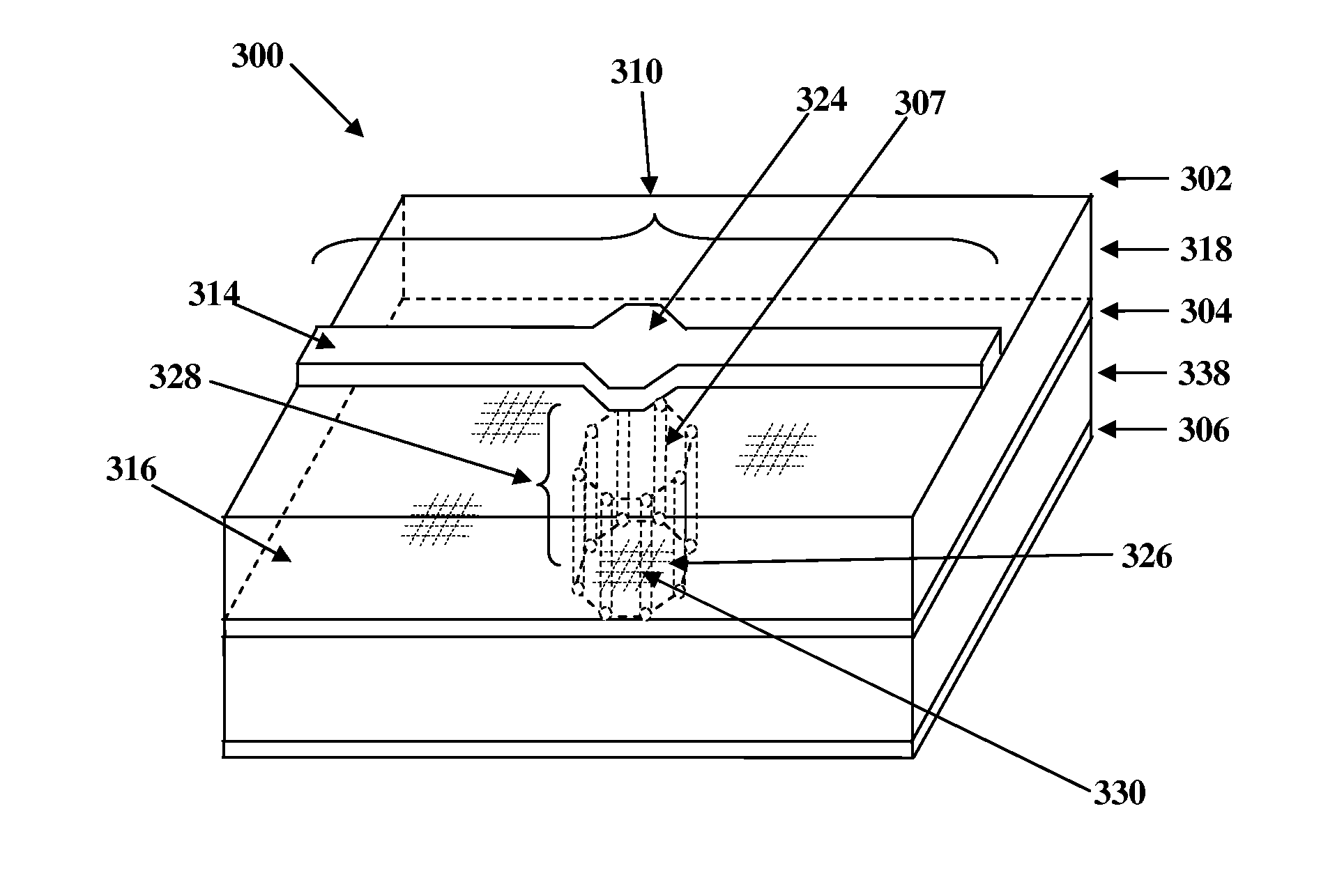
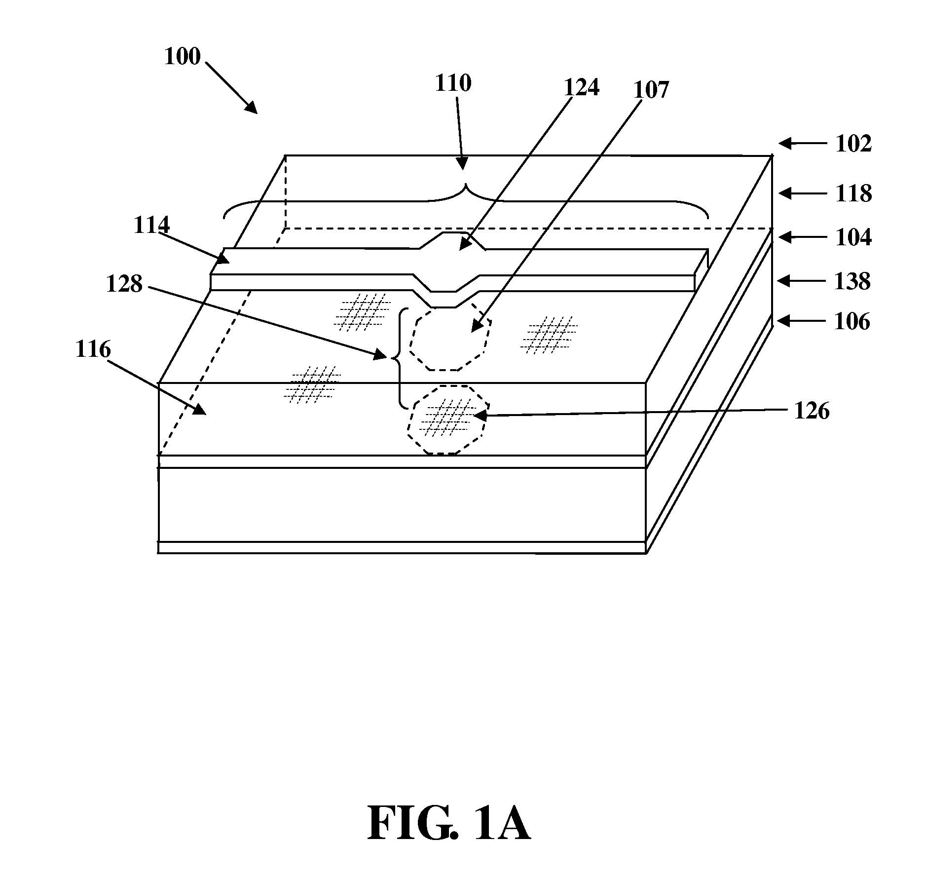
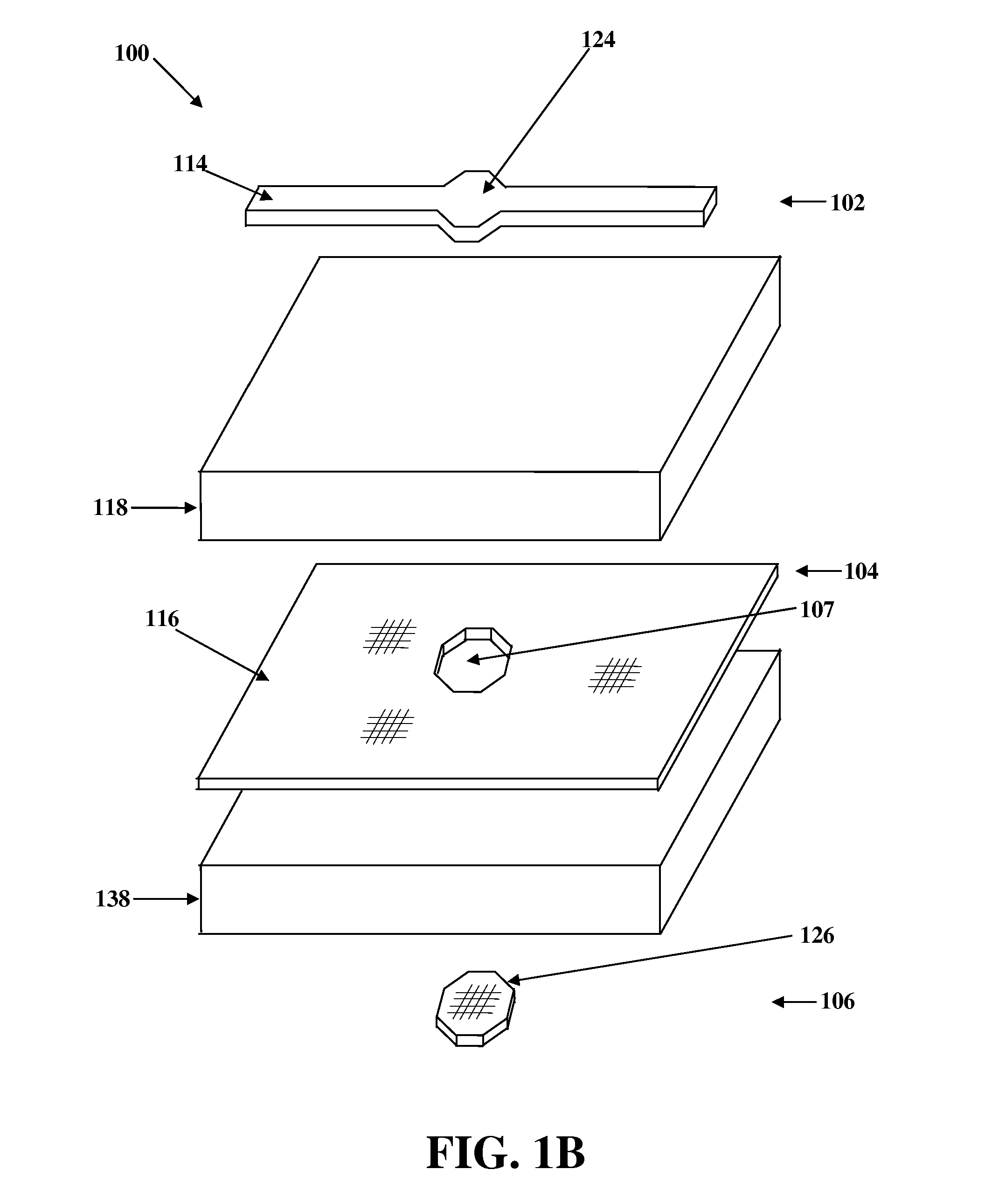
[0058]In an exemplary embodiment of the present invention, a microstrip transmission line is provided on the top layer of a circuit board, the transmission line comprising a 1.46 mm wide and 0.1 mm thick conductive trace overtop of a ground plane on a lower layer of the circuit board. The conductive trace and ground plane are separated by a dielectric having thickness 0.8 mm and relative dielectric constant ∈r=4.2. In accordance with Equation (1), a characteristic impedance of about 50.3 Ohms can be calculated for the example transmission line.

[0059]During functional or in-circuit testing of the circuit board (for example populated or unpopulated with electronic components), it is often necessary to probe the circuit board at several locations. Probing may comprise electrical contact of a spring-loaded test probe to the transmission line conductive trace at one or more predetermined locations, as would be readily understood by a worker skilled in the art. In-circuit test platforms c...


PUM


Abstract

The present invention provides a transmission line portion for a circuit board including a conductive strip and a pad portion including a conductive pad connected to the conductive strip, wherein an impedance discontinuity or mismatch between the transmission line portion and the pad portion is reduced or controlled. Impedance discontinuity or mismatch may be controlled by controlling the dimensions of the pad portion, for example the pad width or distance between pad and ground. A ground pad associated with the pad portion may be provided on a different layer than a ground plane of the transmission line portion. The ground pad and ground plane may be connected by vias. The ground pad may comprise a patterned conductive region, the pattern configured so as to desirably configure impedance of the pad portion. Also provided are a method, circuit board layout, and the like, related to the above.

Description

FIELD OF THE INVENTION[0001]The present invention pertains in general to circuit board design and in particular to circuit boards and methods for matching impedance between a transmission line element and a conductive pad connected thereto.BACKGROUND[0002]Circuit boards, such as multilayer printed circuit boards (PCBs), are widely used in the electronics industry. PCBs typically comprise one or more layers having conductive traces etched onto them, the various layers separated by a dielectric material, with interconnections possible between layers, for example using through-holes or vias. Circuit board design and production is often subject to various, often conflicting, requirements, such as demand for products which are compact, operate at high-speeds, have low costs, and have high reliability. Meeting these requirements presents an ongoing challenge for the industry.[0003]Transmission lines, such as microstrip or striplines, are often used to reliably route high-frequency signals...

Claims


Application Information

Patent Timeline
Patent Type & Authority Applications(United States)
IPC IPC(8): H01P5/02
CPCH01P5/028H01P3/081
Inventor SYAL, ASHISH
Owner NETGEAR INC
Why Eureka
Try Eureka