Encapsulated lens stack

a technology of encapsulated lenses and stacks, which is applied in the field of manufacturing integrated optical devices, can solve the problems of adversely affecting the optical properties of the device, the design of the module is more complicated and costly, and the free access of optical elements on the end faces of the package is subject to damage or contamination, etc., and achieves the effect of easy manufacturing, more freedom of design, and easy manufacturing

Inactive Publication Date: 2011-02-10
HEPTAGON MICRO OPTICS
View PDF13 Cites 26 Cited by
  • Summary
  • Abstract
  • Description
  • Claims
  • Application Information

AI Technical Summary

Benefits of technology

[0019]It is therefore an objective of the present invention to provide a wafer scale package as well as an optical device that overcomes the above mentioned problems and is easier to manufacture than known packages or devices having the same functionality. It is a further objective of the invention to

Problems solved by technology

The following problems arise when manufacturing or handling such packages or devices:
The freely accessible optical elements on the end faces of the package are subject to damage or contamination by dust or an adhesive, especially during the dicing step and/or when further components like a camera or a flash light or other (opto-) electronic components are attached to the wafer scale package or the individual optical device.
Such hoods or cover plates or spacers make the design of the module more complicated and costly.
Especially hoods may also adversely affect the optical properties of the device.
Another problem is associat

Method used


Image

  • Encapsulated lens stack
  • Encapsulated lens stack
  • Encapsulated lens stack

Examples


Embodiment Construction

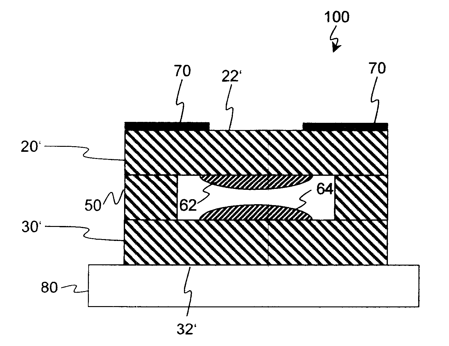
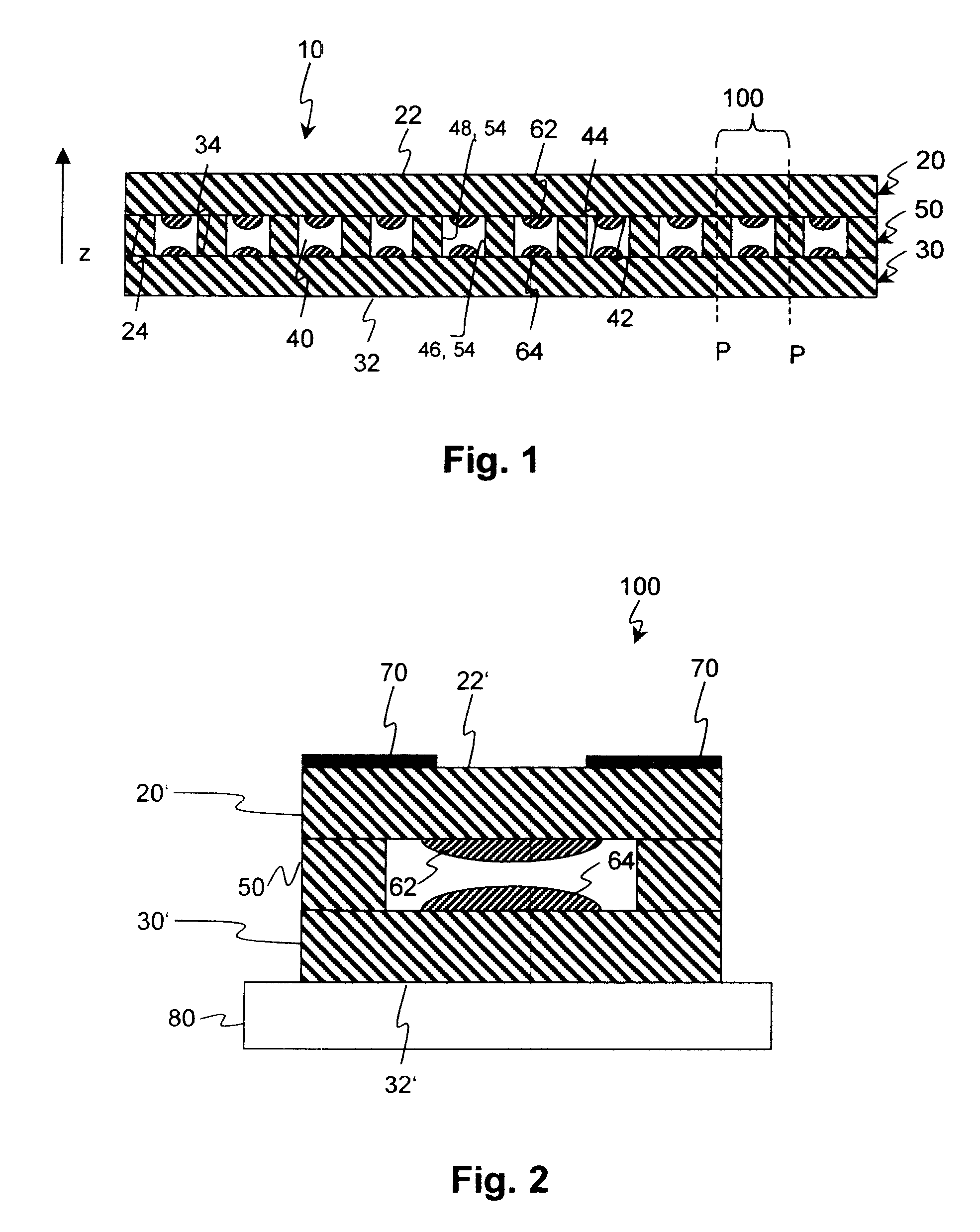
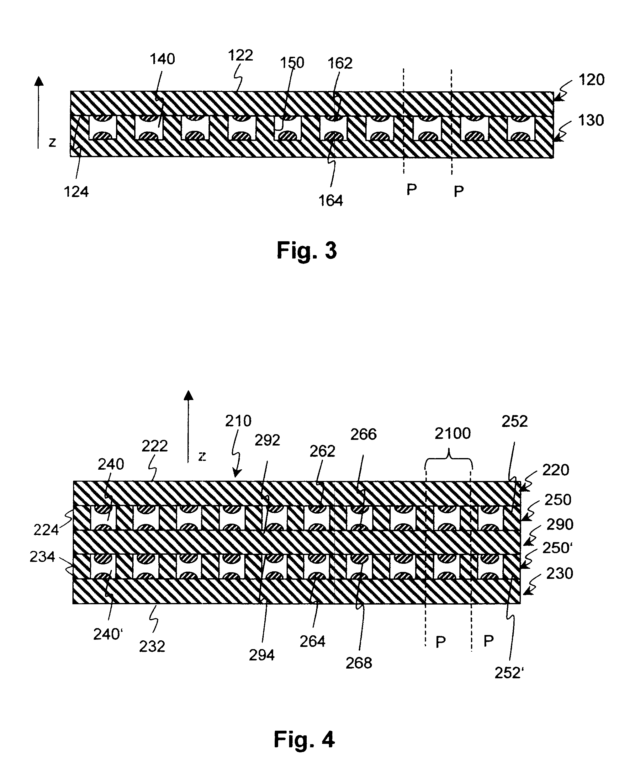
[0058]FIG. 1 shows, purely schematically, an embodiment of a wafer scale package according to the invention 10 with two planar outer substrates 20, 30, which are preferably standard wafers, and a plurality of cavities 40 in between the substrates 20, 30. The outer substrates 20, 30 are stacked in a direction z normal to their main surfaces 22, 24, 32, 34, which is also designated as the axial direction. The substrates 20, 30 are axially spaced by spacer means 50.

[0059]The axial walls 42, 44, i.e. in FIG. 1 the bottom and top walls, of the cavities 40 are constituted by portions of the inner surfaces 24, 34 of the two outer substrates 20, 30. The lateral walls 46, 48 of the cavities 40 are constituted by the corresponding lateral walls 54 of the spacer means 50. The spacer means 50 are constituted by a flat substrate with a plurality of through-holes (spacer matrix), for example, or by individual spacers.

[0060]Optical elements 62, 64 are attached to the inner surfaces 24, 34 of the s...


PUM


Abstract

A wafer scale package includes two or more substrates (wafers) that are stacked in an axial direction and a plurality of replicated optical elements. An optical device includes one or more optical elements. The wafer scale package and the device include one or more cavities that house the optical elements, while the end faces of the package or the device are planar and do not have replicated optical elements thereon. The number of double sided substrates is reduced, and design and manufacture of the optical device is improved.

Description

BACKGROUND OF THE INVENTION[0001]1. Field of the Invention[0002]The invention is in the field of manufacturing integrated optical devices with two or more optical elements, e.g. refractive and / or diffractive lenses, in a well defined spatial arrangement on wafer scale by means of a replication process. Such integrated optical devices are, for example, camera devices, optics for camera devices, or collimating optics for flash lights, especially for camera mobile phones. More concretely, the invention relates to a wafer scale package comprising two or more substrates (wafers) that are stacked in an axial direction and have a plurality of replicated optical elements. The invention further relates to an optical device, e.g. a camera or a collimating optics therefor, comprising two or more replicated optical elements and optionally also electro-optical components, to a method for production of such a wafer scale package, and to a method of manufacturing a plurality of optical elements.[0...

Claims


Application Information

Patent Timeline
IPC IPC(8): H01L33/58H01L31/0232H01L31/18
CPCG02B3/0062G02B7/02H04N5/2257H01L27/14685H01L2924/16235H01L27/14627B29D11/00307H04N23/57
Inventor ROSSI, MARKUSRUDMANN, HARTMUTKETTUNEN, VILLE
Owner HEPTAGON MICRO OPTICS
Why Eureka
Try Eureka