Method and system for powering and cooling semiconductor layers

a technology of powering and cooling semiconductor layers, applied in the direction of semiconductor laser arrangements, semiconductor lasers, lasers, etc., can solve the problems of challenging precise current regulation of power conditioning electronics, and achieve the effects of reducing system size and cost, enhancing reliability, and reducing system cos

Active Publication Date: 2011-03-03
LAWRENCE LIVERMORE NAT SECURITY LLC
View PDF14 Cites 11 Cited by
  • Summary
  • Abstract
  • Description
  • Claims
  • Application Information

AI Technical Summary

Benefits of technology

[0009]Numerous benefits are achieved by way of the present invention over conventional techniques. For example, the present systems provide integrated cooling of both semiconductor laser pumps and components of the electrical pulse generator used in driving the semiconductor laser pumps. Mounting of components of the electrical pulse generator in thermal communication with the cooling structure used to cool the semiconductor laser pumps reduces the system size and cost. Embodiments of the present invention provide a diode laser pump tile that reduces system cost and enhances reliability by integrating the pulse...

Problems solved by technology

As a result, precise current regulation usi...

Method used


Image

  • Method and system for powering and cooling semiconductor layers
  • Method and system for powering and cooling semiconductor layers
  • Method and system for powering and cooling semiconductor layers

Examples


Embodiment Construction

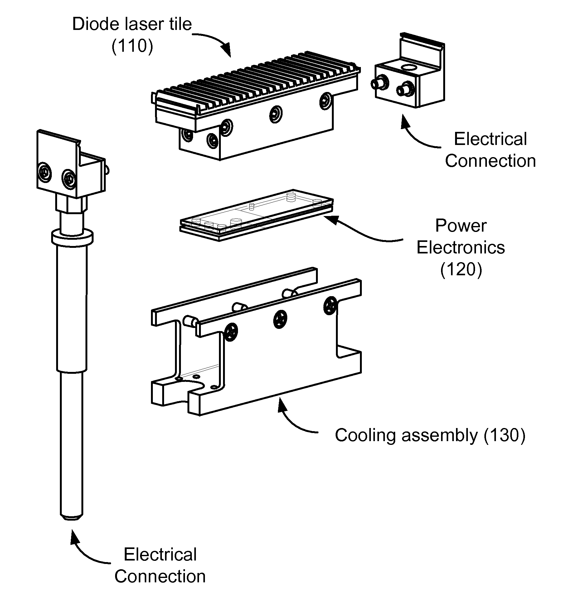
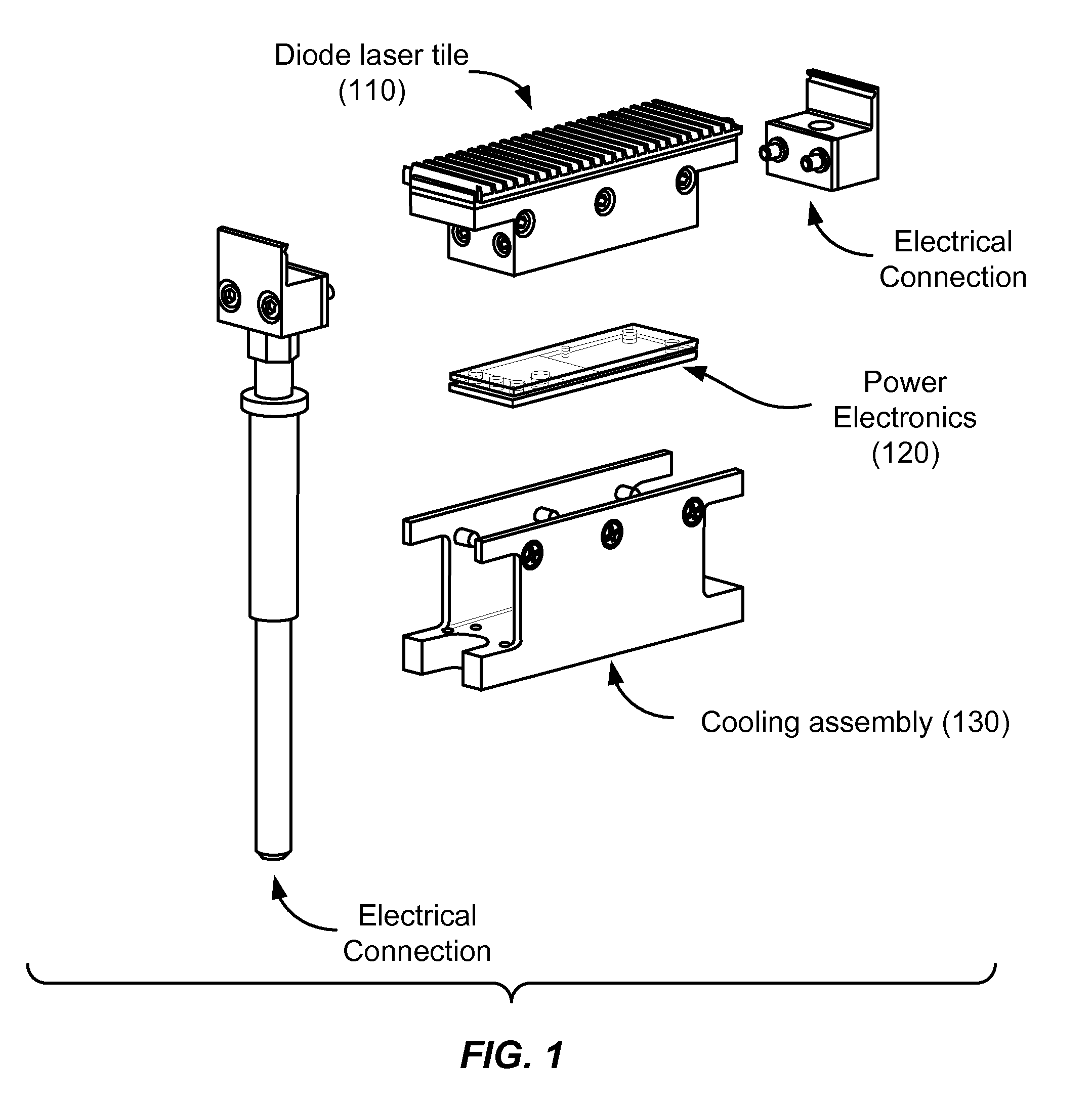
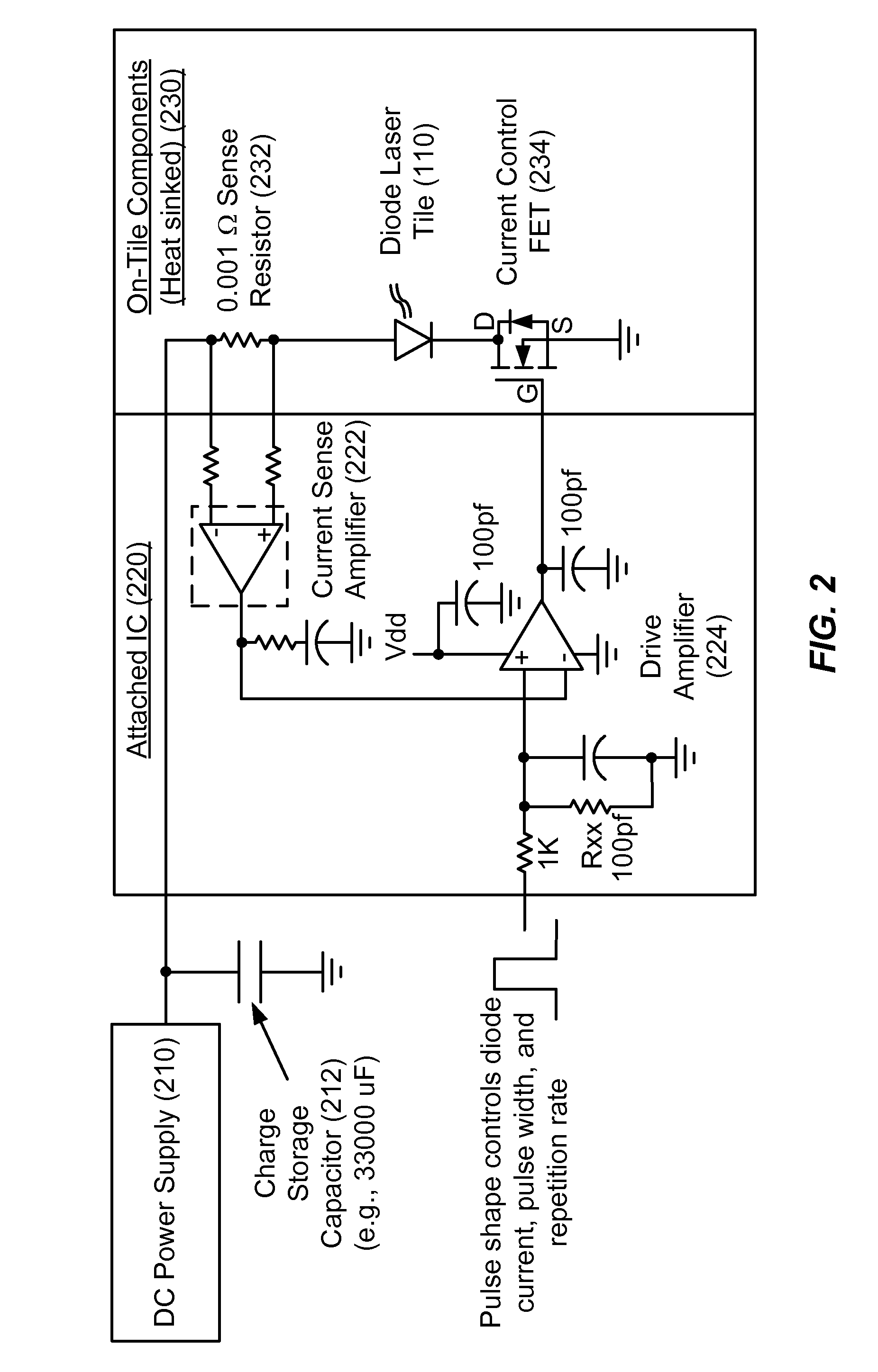
[0020]Typically, power conditioning electronics used for high power diode laser (i.e., semiconductor laser) pumps are either actively cooled or limited in their duty cycle. As an example, the power conditioning electronics used to drive the diode laser pumps used in the Mercury laser at Lawrence Livermore National Laboratory (LLNL) were actively cooled. In other laser systems, the control of the duty factor of the power conditioning electronics necessitated by thermal concerns may limit the operational characteristics of the laser.

[0021]Embodiments of the present invention integrate one or more components of the power conditioning system and the diode monitoring system with the diode package, thereby providing benefits not available using conventional systems. These benefits may include: (1) eliminating the need for a separate cooling system for the power conditioning electronics; (2) eliminating the duty factor limitation due to thermal constraints associated with the power conditi...


PUM


Abstract

A semiconductor laser system includes a diode laser tile. The diode laser tile includes a mounting fixture having a first side and a second side opposing the first side and an array of semiconductor laser pumps coupled to the first side of the mounting fixture. The semiconductor laser system also includes an electrical pulse generator thermally coupled to the diode bar and a cooling member thermally coupled to the diode bar and the electrical pulse generator.

Description

CROSS-REFERENCES TO RELATED APPLICATIONS[0001]The present application claims benefit under 35 U.S.C. §119(e) of U.S. Provisional Patent Application No. 61 / 239,569, filed on Sep. 3, 2009, entitled “Method and System for Powering and Cooling Semiconductor Lasers,” the disclosure of which is hereby incorporated by reference in its entirety for all purposes.STATEMENT AS TO RIGHTS TO INVENTIONS MADE UNDER FEDERALLY SPONSORED RESEARCH OR DEVELOPMENT[0002]The United States Government has rights in this invention pursuant to Contract No. DE-AC52-07NA27344 between the United States Department of Energy and Lawrence Livermore National Security, LLC.BACKGROUND OF THE INVENTION[0003]High average power diode pumped lasers are currently being used in or designed into an increasing number of laser systems. As the optical output power of these high average power diode pumped lasers increases, the input optical power required from the diode laser pumps typically increases as well. Since the efficien...

Claims


Application Information

Patent Timeline
IPC IPC(8): H01S3/04H01S3/102H01S5/40
CPCH01S5/02248H01S5/02407H01S5/02438H01S5/4025H01S5/06808H01S5/4018H01S5/0428H01S5/06216H01S5/02325
Inventor TELFORD, STEVEN J.LADRAN, ANTHONY S.
Owner LAWRENCE LIVERMORE NAT SECURITY LLC
Why Eureka
Try Eureka