Nanostructured substrates for surface enhanced raman spectroscopy (SERS) and detection of biological and chemical analytes by electrical double layer (EDL) capacitance

a technology of electrical double layer and nanostructure, applied in the field of nanostructured substrates for surface enhanced raman spectroscopy and detection of biological and chemical analytes by electrical double layer (edl) capacitance, can solve the problems of inability to achieve a large number of hot spots, inability to achieve significant progress toward detailed understanding of edl structure, and inability to utilize this phenomenon for practical applications. to achieve the effect of enhancing the radiation scattered by the analy

Inactive Publication Date: 2011-03-03
CLEMSON UNIV RES FOUND
View PDF7 Cites 103 Cited by
  • Summary
  • Abstract
  • Description
  • Claims
  • Application Information

AI Technical Summary

Benefits of technology

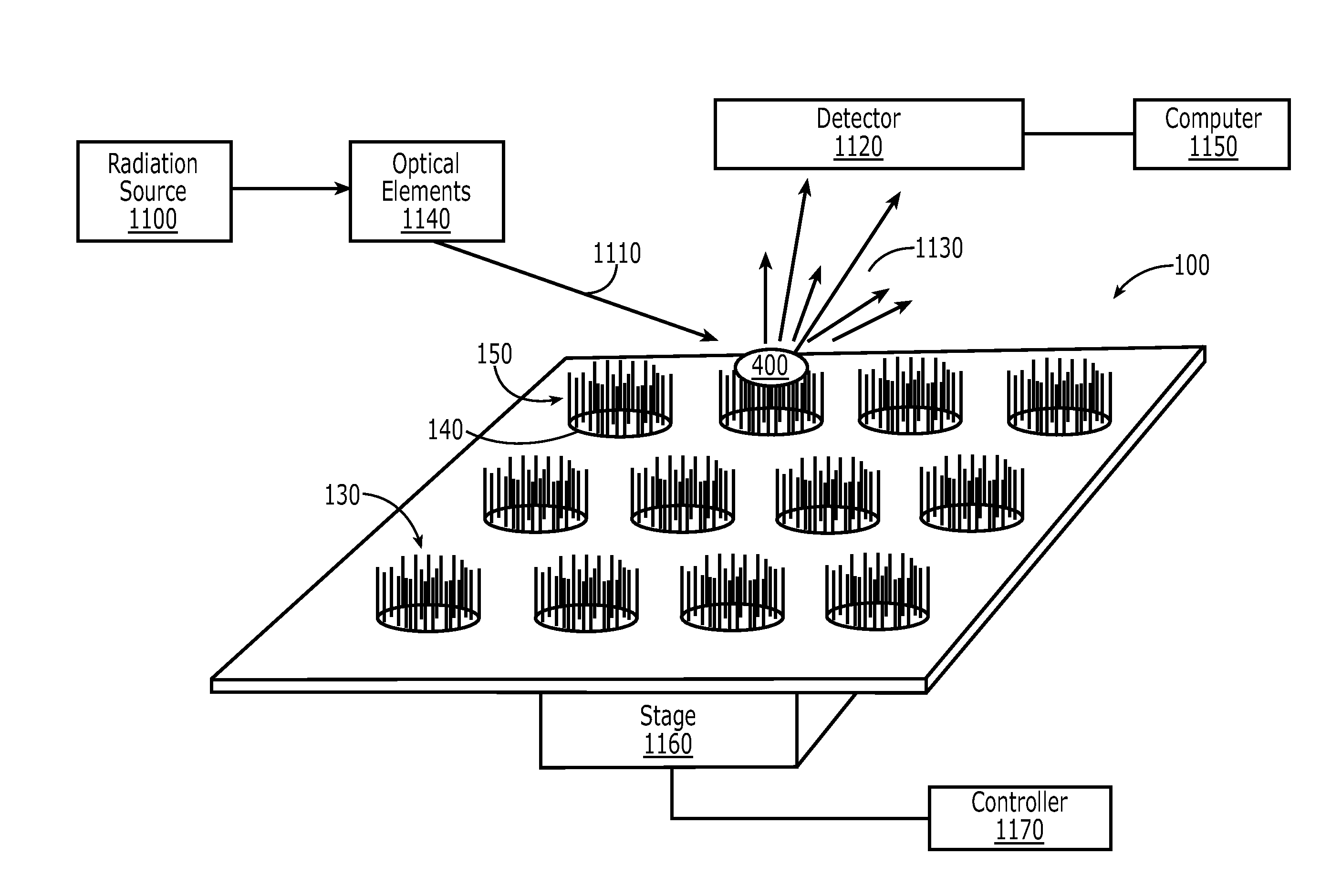
[0013]Also provided according to embodiments of the invention are methods of detecting an analyte by Surface Enhanced Raman Spectroscopy that include (i) binding at least one analyte to a nanostructured surface according to an embodiment of the invention; (ii) irradiating the at least one analyte bound to the nanostructured surface; and (iii) detecting radiation scattered by the at least one analyte. In some embodiments, binding of the at least one analyte to the at least one metallic nanopillar island may include electrically charging the metallic nanopillars of the at least one metallic nanopillar island; trapping the at least one analyte within the metallic nanopillars; and discharging the metallic nanopillars. Additionally, in some embodiments, the methods may further include correlating the radiation scattered by the at least one analyte with a chemical structure of the at least one analyte. Furthermore, in some embodiments, the metallic nanopillars may enhance the radiation scattered by the analyte by an enhancement factor in a range of about 108 to about 1015.

Problems solved by technology

Although these nano features are typically spread over an entire surface, the number of hot spots attainable may be limited and inconsistent.
Aside from some recent efforts made to incorporate nanostructures to a surface to achieve super charge capacitors, there has not been significant progress toward detailed understanding of the EDL structure, or toward utilizing this phenomenon for practical applications.

Method used


Image

  • Nanostructured substrates for surface enhanced raman spectroscopy (SERS) and detection of biological and chemical analytes by electrical double layer (EDL) capacitance
  • Nanostructured substrates for surface enhanced raman spectroscopy (SERS) and detection of biological and chemical analytes by electrical double layer (EDL) capacitance
  • Nanostructured substrates for surface enhanced raman spectroscopy (SERS) and detection of biological and chemical analytes by electrical double layer (EDL) capacitance

Examples


example

[0117]Provided below is an example of a method for forming a nanostructured surface according to an embodiment of the invention:[0118]Step 1: Sample preparation: A silicon wafer or a glass slide is cleaned and then coated with a thin layer of titanium (10 nm) followed by a layer of gold (5-10 nm) and a thick layer of aluminum (1.5 μm) using an e-beam evaporator. The Al layer is then electropolished in a 9:1 ethanol to water solution to remove to remove any oxide layer prior to anodization. See FIG. 5A.[0119]Step 2: Anodization: Anodization in 0.3 M oxalic acid at 5° C. at 40 V is performed until it reaches the gold layer through the monitoring of the anodization current. See FIG. 5B.[0120]Step 3: Electrodeposition: Silver nanopillars are formed through electrodeposition into the nanopores in a silver potassium cyanide bath at 5 mA / cm2 for 50 s. See FIG. 5C.[0121]Step 4: Alumina removal: The alumina template is removed by dipping in 2.0M NaOH solution for about 20 minutes. See FIG. 5...


PUM

PropertyMeasurementUnit
inter-island distanceaaaaaaaaaa
widthaaaaaaaaaa
distanceaaaaaaaaaa

Abstract

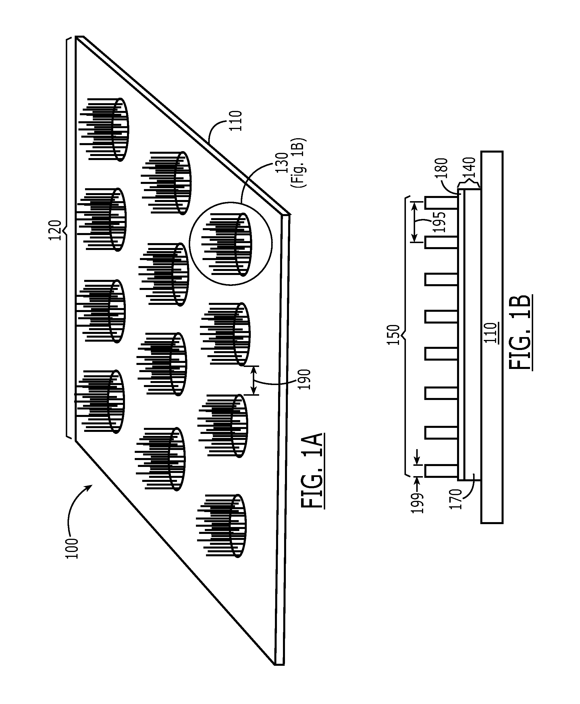
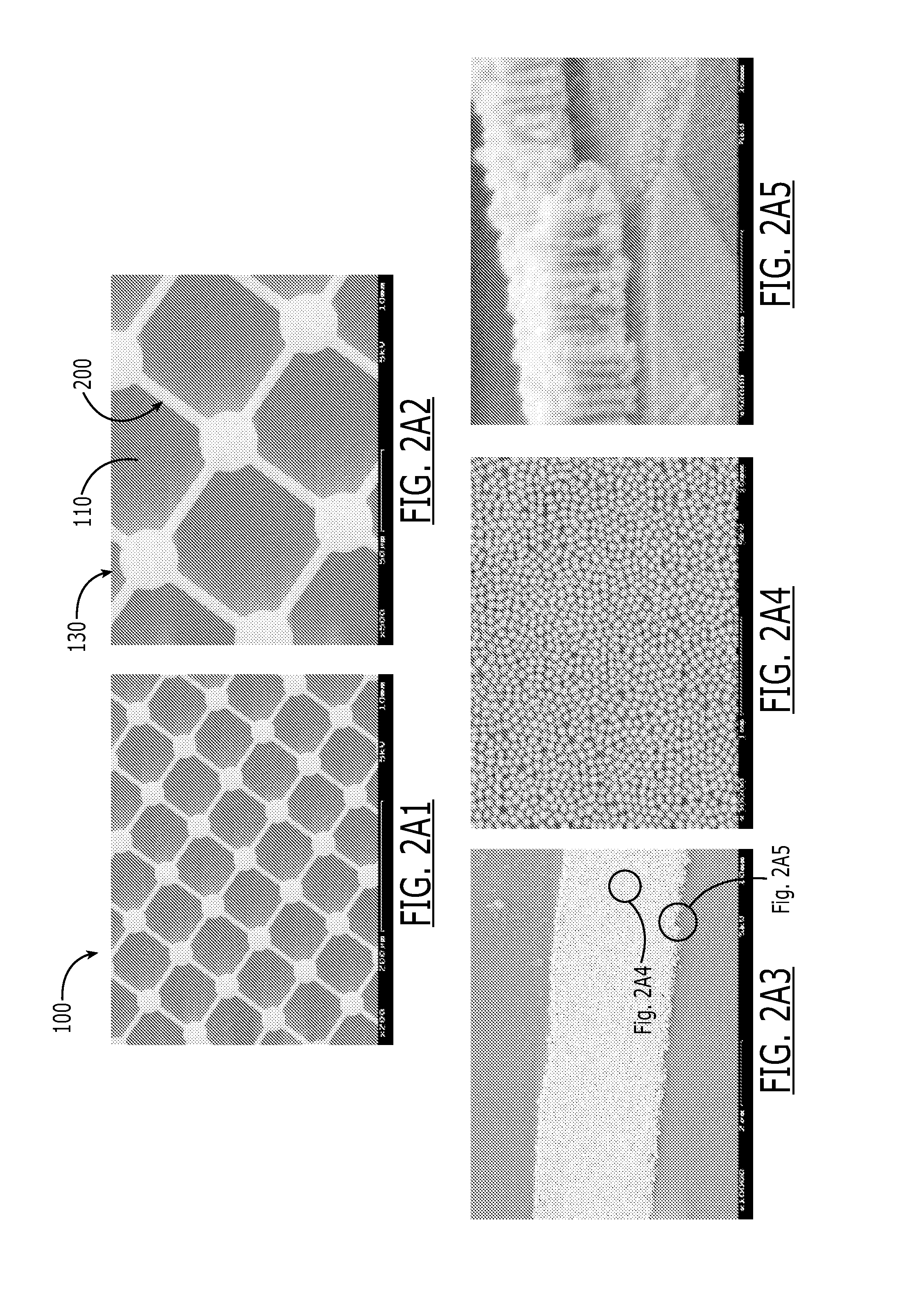
Provided according to embodiments of the invention are nanostructured surfaces that include a substrate; and an array of metallic nanopillar islands on the substrate, wherein each metallic nanopillar island includes a metal base layer on the substrate and a plurality of metallic nanopillars on the metal base layer, and wherein portions of the substrate between adjacent metallic nanopillar islands are free of the metal base layer. Also provided according to some embodiments of the invention are nanostructured surfaces that include a non-conductive substrate; and at least one nanoelectrode defined within the non-conductive substrate, wherein the at least one nanoelectrode is sized and/or shaped to immobilize an analyte or a probe molecule. Also provided are apparatuses and methods for SERS and detection of analytes or biological binding by EDL capacitance.

Description

CROSS-REFERENCE TO RELATED APPLICATIONS[0001]This application claims priority from U.S. Provisional Application Ser. No. 61 / 237,034, filed Aug. 26, 2009, and U.S. Provisional Application Ser. No. 61 / 310,875, filed Mar. 5, 2010, the disclosures of which are hereby incorporated by reference herein in their entirety.FIELD OF THE INVENTION[0002]The present invention relates to surfaces having nanometer scaled structures. The present invention also relates to surfaces and methods for Surface Enhanced Raman spectroscopy (SERS). The present invention also relates to surfaces and methods for detection of analytes and biological interfacing by electrical double layer (EDL) capacitance.BACKGROUND OF THE INVENTION[0003]Surface-enhanced Raman Spectroscopy (SERS) is a sensing technique that may be capable of providing relatively fast, specific and label-free detection of spectroscopic fingerprints of molecules adsorbed on metal surfaces. It has been shown that a substantial Raman enhancement may...

Claims


Application Information

Patent Timeline
Patent Type & Authority Applications(United States)
IPC IPC(8): C40B30/04C40B40/18C40B60/12
CPCB01J19/0046B01J2219/00509B01J2219/00533B01J2219/00585B01J2219/00596B01J2219/00605G01N33/553B01J2219/00659B01J2219/00704B82Y30/00B82Y40/00G01N21/658G01N33/5438B01J2219/00653C25D11/045
Inventor ZHANG, GUIGEN
Owner CLEMSON UNIV RES FOUND
Why Eureka
Try Eureka