Supercharge Your Innovation With Domain-Expert AI Agents!

Logic Chip, Method and Computer Program for Providing a Configuration Information for a Configurable Logic Chip

a logic chip and configuration information technology, applied in the field of logic chips and computer programs, can solve the problems of significant challenges in the complexity of logic circuits, logic chips and logic systems is steadily increasing, and the design of logic circuits is challenging

Inactive Publication Date: 2011-03-03
FRIEDRICH ALEXANDER UNIV ERLANGEN NUERNBERG
View PDF1 Cites 9 Cited by
  • Summary
  • Abstract
  • Description
  • Claims
  • Application Information

AI Technical Summary

Benefits of technology

The patent describes a logic chip with individually addressable resource blocks, such as modules or slots, that can be connected to a bus with multiple bus information lines. The chip also includes a configuration information that describes the connections between the resource blocks and the bus information lines. The technical effect of this invention is to provide a flexible and efficient way to connect the logic circuitry of the chip's resource blocks to the bus, allowing for the efficient use of space and improved performance.

Problems solved by technology

The design of logic circuits has been a challenging task.
However, at present, the complexity of logic circuits, logic chips and logic systems is steadily increasing.
This brings along significant challenges in the design of such logic circuits.
Also, with increasing complexity of the logic circuits, it is getting more and more difficult to provide an efficient way of interconnecting different logic blocks.
One important issue of this work is the interfacing of hardware accelerators to on-chip buses (OCBs) and to the static system containing typically a CPU, the memory, and the I / O interface modules.
This approach does not allow a direct connection to I / O-peripherals connected to the OCB.
Both approaches do not allow a module to directly access any memory of the system.
The large multiplexers have also significant propagation delays leading to decreased throughputs when using circuit switching.
This approach necessitates a significant amount of area on the FPGA around the modules in order to build the routing because there is no technique available to share the routing wires inside the templates for building multiple routing tracks.
As modules are obstacles for this kind of routing, the area necessitated for routing cannot be used to implement the module's logic.
We can conclude that packet routing produces an enormous overhead when implemented on FPGAs.
However, newer FPGA architectures have no support for tristate wires and none of these approaches deal efficiently with dedicated signals, e.g., interrupt lines and chip select signals.
The main drawback of this solution is that all modules have to fit into such a resource area and that the resource areas could not be shared by multiple modules, even if the logic of multiple modules would fit into the same resource area.

Method used


Image

  • Logic Chip, Method and Computer Program for Providing a Configuration Information for a Configurable Logic Chip
  • Logic Chip, Method and Computer Program for Providing a Configuration Information for a Configurable Logic Chip
  • Logic Chip, Method and Computer Program for Providing a Configuration Information for a Configurable Logic Chip

Examples


Embodiment Construction

[0136]Embodiments according to the invention will subsequently be described taking reference to the enclosed FIGS.

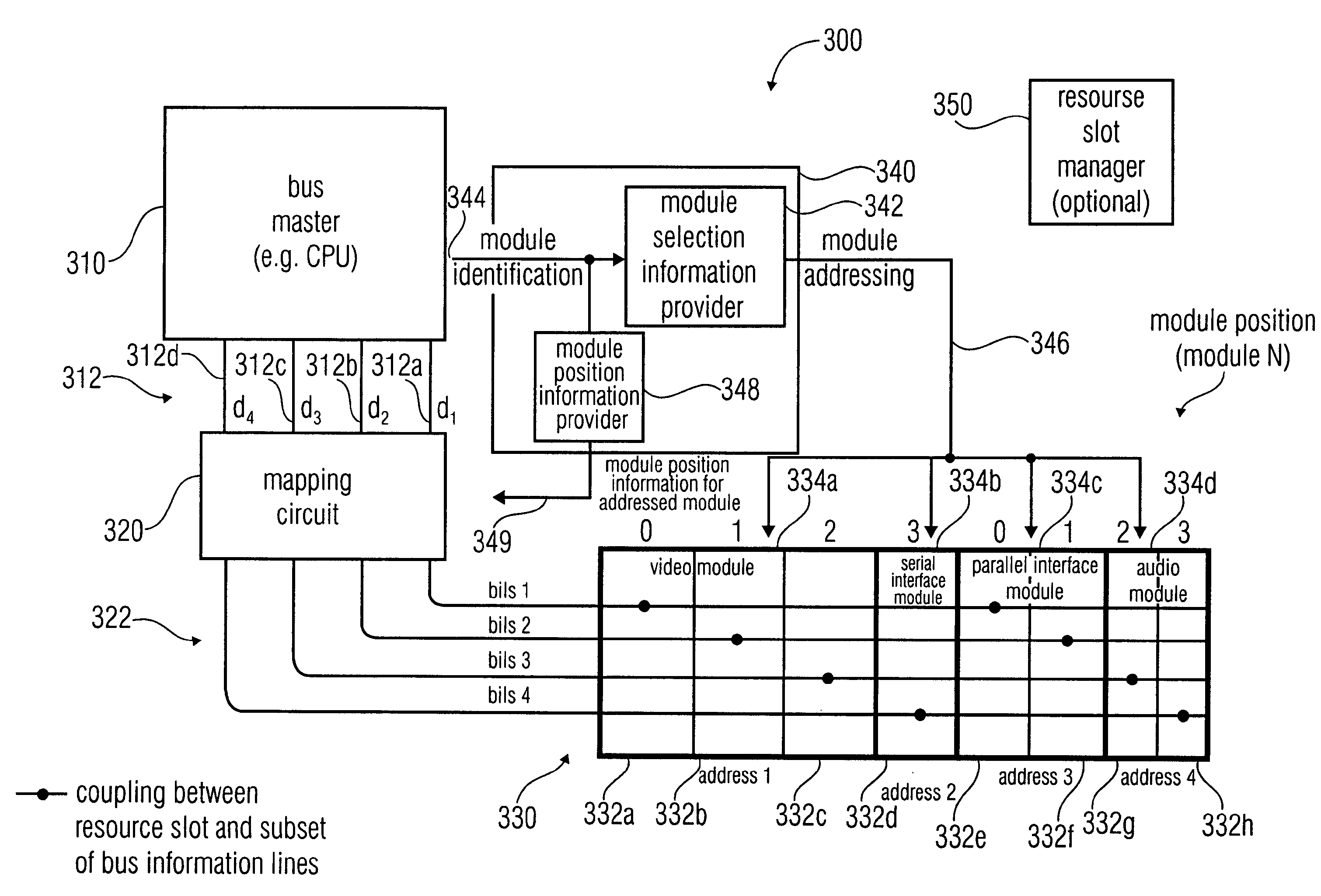
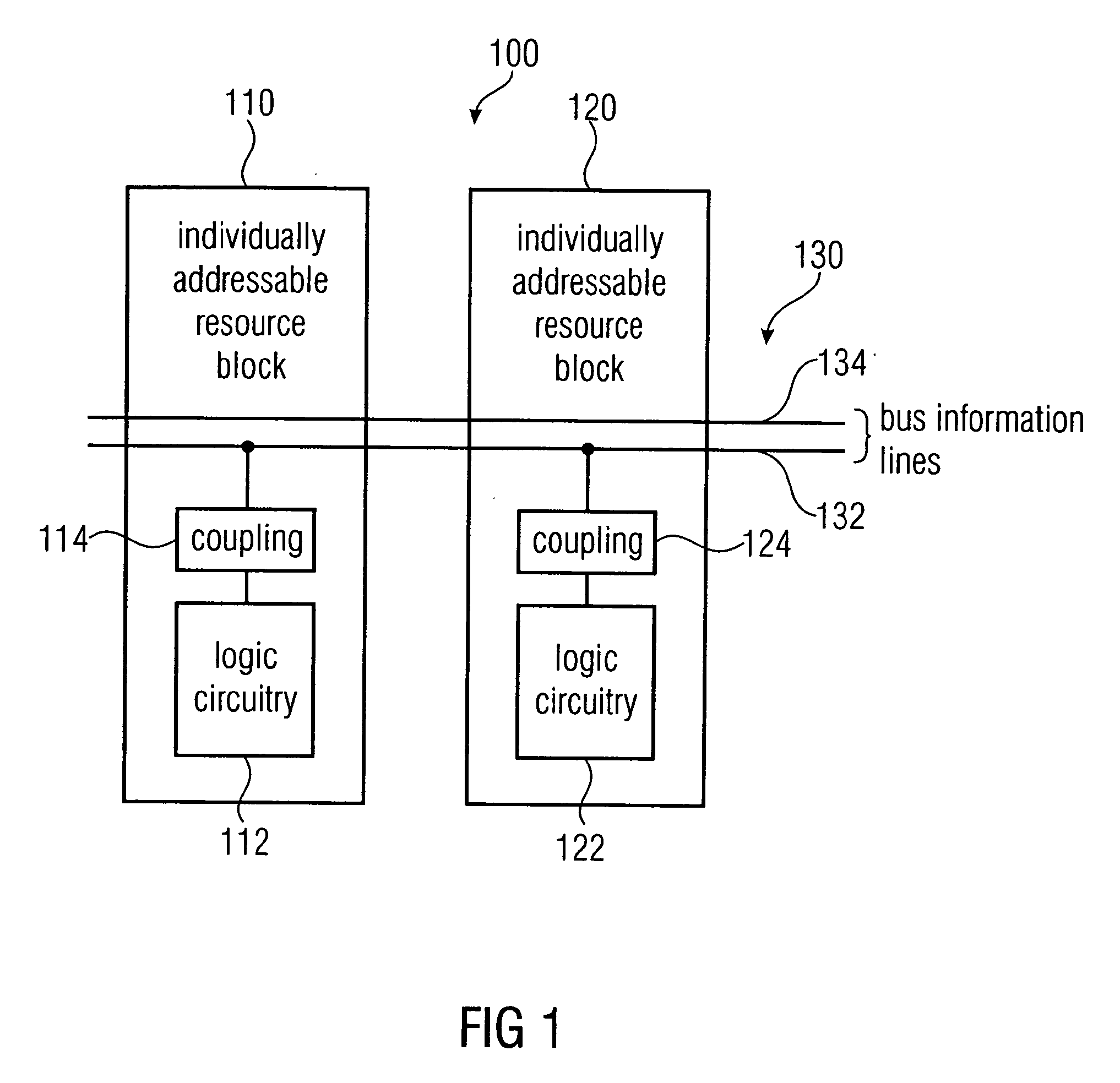
[0137]FIG. 1 shows a block schematic diagram of a logic chip, according to an embodiment of the invention. The logic chip is designed in its entirety with 100. The logic chip comprises a plurality of individually-addressable resource blocks (or resource slots), for example, a first individually-addressable resource block 110 and a second individually-addressable resource block 120. Each of the individually-addressable resource blocks comprises logic circuitry 112, 122.

[0138]It should be noted that the individually-addressable resource blocks may, for example, be individually-addressable resource slots. Alternatively, the individually-addressable resource blocks may be modules, wherein a module may comprise a plurality of resource slots. However, a mixed configuration may be used, wherein the first individually-addressable resource block may be an individually-addressable...


PUM


Abstract

A logic chip has a plurality of individually-addressable resource blocks, each comprising logic circuitry. The logic chip also has a bus comprising a plurality of bus information lines. A first of the resource blocks has a coupling between a first strict sub-set of the bus information lines and the logic circuitry of the first resource block. A second of the resource blocks, which is adjacent to the first resource block, has a coupling between a second strict sub-set of the bus information lines and the logic circuitry of the second resource blocks. The first and second sub-sets have different bus lines.

Description

CROSS-REFERENCE TO RELATED APPLICATIONS[0001]This application is a National Phase of PCT / EP2008 / 007343 filed 8 Sep. 2008, which claims priority from German Patent Application No. 07017975.9, which was filed on 13 Sep. 2007, and is incorporated herein in its entirety by reference.BACKGROUND OF THE INVENTION[0002]Some embodiments according to the invention are related to a logic chip and to a method and computer program for providing a configuration information for a configurable logic chip.[0003]Some embodiments according to the invention are related to a logic chip, a logic system and a method and computer program for designing a logic chip.[0004]Some embodiments according to the invention are related to efficient re-configurable on-chip buses.[0005]Some embodiments according to the invention are related to further developments regarding efficient re-configurable on-chip buses.[0006]Some embodiments according to the invention are related to efficient re-configurable on-chip buses fo...

Claims


Application Information

Patent Timeline
Patent Type & Authority Applications(United States)
IPC IPC(8): G06F13/40
CPCG06F15/7867G06F15/8015H03K19/17796H03K19/17736H03K19/17748G06F17/5054G06F30/34
Inventor KOCH, DIRKSTREICHERT, THILOHAUBELT, CHRISTIANTEICH, JUERGEN
Owner FRIEDRICH ALEXANDER UNIV ERLANGEN NUERNBERG
Features
  • R&D
  • Intellectual Property
  • Life Sciences
  • Materials
  • Tech Scout
  • Unparalleled Data Quality
  • Higher Quality Content
  • 60% Fewer Hallucinations
Learn More