Light-Emitting Element, Light-Emitting Device, and Method for Manufacturing the Same

a technology of light-emitting elements and manufacturing methods, which is applied in the direction of thermoelectric devices, organic semiconductor devices, other domestic articles, etc., can solve the problems of reducing the reliability of light-emitting elements, reducing the emission efficiency, and reducing the efficiency of emission, so as to achieve high emission efficiency and reliable effect, the luminance is not easily decreased during operation

Active Publication Date: 2011-03-10
SEMICON ENERGY LAB CO LTD
View PDF42 Cites 65 Cited by
  • Summary
  • Abstract
  • Description
  • Claims
  • Application Information

AI Technical Summary

Benefits of technology

[0036]With the present invention, a light-emitting element with high emission efficiency can be provided. Further, a highly reliable light-emitting element whose luminance is not decreased easily during operation can be provided. Furthermore, a light-emitting element which is driven at a low voltage can be provided.

Problems solved by technology

Therefore, it is difficult to achieve and maintain the balance of carriers.
Carriers which have passed from one side of the light-emitting layer to the other side without recombination cause the decrease in emission efficiency and the decrease in reliability of the light-emitting element.
Further, holes which have passed through the light-emitting layer and have reached the electron-transport layer might oxidize the electron-transport layer, resulting in deterioration in the electron-transport layer.
In a similar manner, electrons which have passed through the light-emitting layer and have reached the hole-transport layer might reduce the hole-transport layer, resulting in deterioration in the hole-transport layer.
However, there is a case where carriers which are confined by this method serve as quenchers, resulting in the decrease in emission efficiency.
Since the cationic species often serve as quenchers, the emission efficiency of the element is diminished.

Method used


Image

  • Light-Emitting Element, Light-Emitting Device, and Method for Manufacturing the Same
  • Light-Emitting Element, Light-Emitting Device, and Method for Manufacturing the Same
  • Light-Emitting Element, Light-Emitting Device, and Method for Manufacturing the Same

Examples


embodiment 1

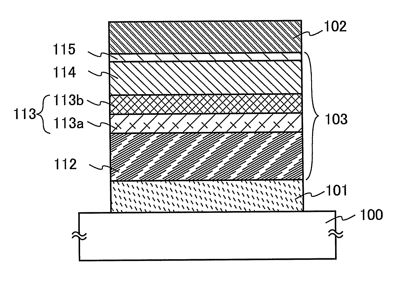
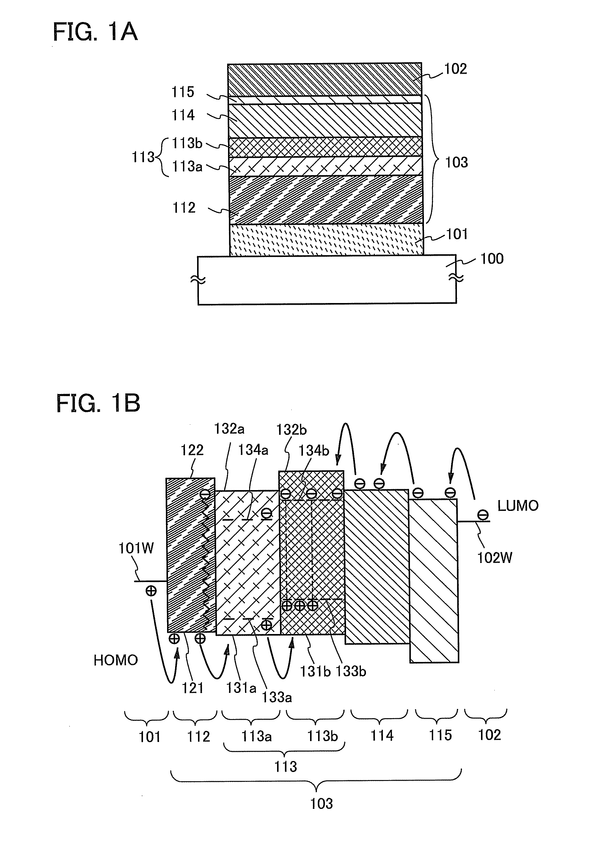
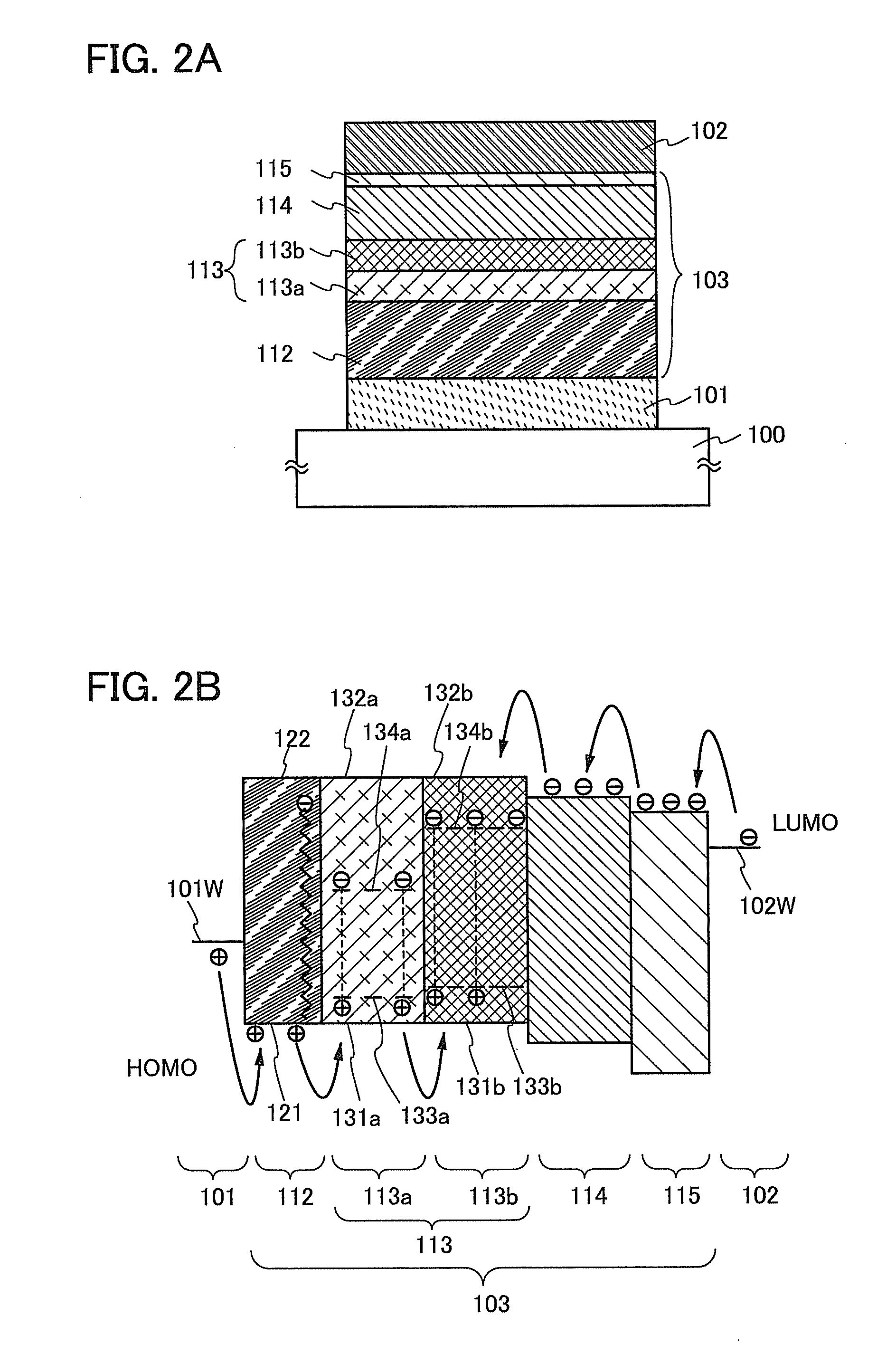
[0065]A light-emitting element which is described in this embodiment includes at least a first light-emitting layer whose one side is in contact with a hole-transport layer and a second light-emitting layer which is in contact with the other side of the first light-emitting layer. Both the first light-emitting layer and the second light-emitting layer contain a bipolar host material and a guest material which is a light-emitting material. The guest material contained in the first light-emitting layer has a lower ability for capturing a hole than the guest material contained in the second light-emitting layer; therefore, the hole-transport property of the first light-emitting layer is higher than that of the second light-emitting layer. As a result, holes are transported into a region apart from the hole-transport layer, and a recombination region of holes and electrons are formed widely in the light-emitting layers. Furthermore, an anti-reducing material is contained in the hole-tra...

embodiment 2

[0147]A light-emitting element illustrated in this embodiment includes at least a first light-emitting layer whose one side is in contact with a hole-transport layer, and a second light-emitting layer in contact with the other side of the first light-emitting layer. Both the first light-emitting layer and the second light-emitting layer contain a bipolar host material and a guest material which is a light-emitting material. The guest material contained in the first light-emitting layer has a low ability for capturing a hole than the guest material contained in the second light-emitting layer; therefore, the hole-transport property of the first light-emitting layer is higher than that of the second light-emitting layer. As a result, holes are transported to a region apart from the hole-transport layer, and a recombination region of holes and electrons is formed widely in the light-emitting layers. Emission colors of the light-emitting material contained in the first light-emitting la...

embodiment 3

[0182]A light-emitting element which is illustrated in this embodiment includes at least a first light-emitting layer whose one side is in contact with a hole-transport layer, a second light-emitting layer in contact with the other side of the first light-emitting layer, and a third light-emitting layer in contact with a side of the second light-emitting layer on a cathode side. The first light-emitting layer, the second light-emitting layer, and the third light-emitting layer each contain a bipolar host material and a guest material which is a light-emitting material. The guest material contained in the first light-emitting layer has a lower ability for capturing a hole than the guest material contained in the second light-emitting layer, and the guest material contained in the second light-emitting layer has a lower ability for capturing a hole than the guest material contained in the third light-emitting layer. The hole-transport property of the first light-emitting layer is high...


PUM


Abstract

Disclosed is a light-emitting element which includes a first light-emitting layer over and in contact with a hole-transport layer and a second light-emitting layer over and in contact with the first light-emitting layer. The first and the second light-emitting layers contain a bipolar host material and an emissive guest material. The guest material in the first light-emitting layer has a lower ability for capturing a hole than a guest material in the second light-emitting layer; therefore, the hole-transport property of the first light-emitting layer can be controlled to be higher than that of the second light-emitting layer. The difference in hole-transport property between the first and second light-emitting layers allows a recombination region to be widely spread in the light-emitting layers. An anti-reducing material may be provided in the hole-transport layer, which prevents the hole-transport layer from being reduced by electrons which fail to undergo recombination in the light-emitting layers.

Description

TECHNICAL FIELD[0001]The present invention relates to a light-emitting element, a light-emitting device, and a manufacturing method thereof.BACKGROUND ART[0002]In recent years, research and development have been extensively conducted on light-emitting elements using electroluminescence. Such a light-emitting element has a structure where a layer containing a material with a light-emitting property is interposed between a pair of electrodes. By application of a voltage between the pair of electrodes, light can be emitted from the material with a light-emitting property.[0003]Characteristic features of the light-emitting element using electroluminescence can be found in its advantages in being manufactured to be thin and lightweight and having very fast response time. There are various possible applications of such a self-luminous light-emitting element. For example, the light-emitting element is preferably used for a flat panel display because it has advantages such as high visibilit...

Claims


Application Information

Patent Timeline
Patent Type & Authority Applications(United States)
IPC IPC(8): H01L51/54
CPCH01L51/006H01L51/0072H01L51/0081H01L51/504H01L51/5048H01L2251/552H01L51/5012H10K85/633H10K85/6572H10K85/324H10K50/13H10K50/14H10K50/11H10K2101/30Y10S428/917
Inventor SHITAGAKI, SATOKOSEO, SATOSHI
Owner SEMICON ENERGY LAB CO LTD
Why Eureka
Try Eureka