Advanced electronic ballasts
a technology of electronic ballasts and ballasts, applied in the field of electronic ballasts, can solve the problems of high cost, large amount of filtering, and high frequency of mains, and achieve the effect of occupying a small circuit space and being easy to implemen
- Summary
- Abstract
- Description
- Claims
- Application Information
AI Technical Summary
Benefits of technology
Problems solved by technology
Method used
Image
Examples
first embodiment
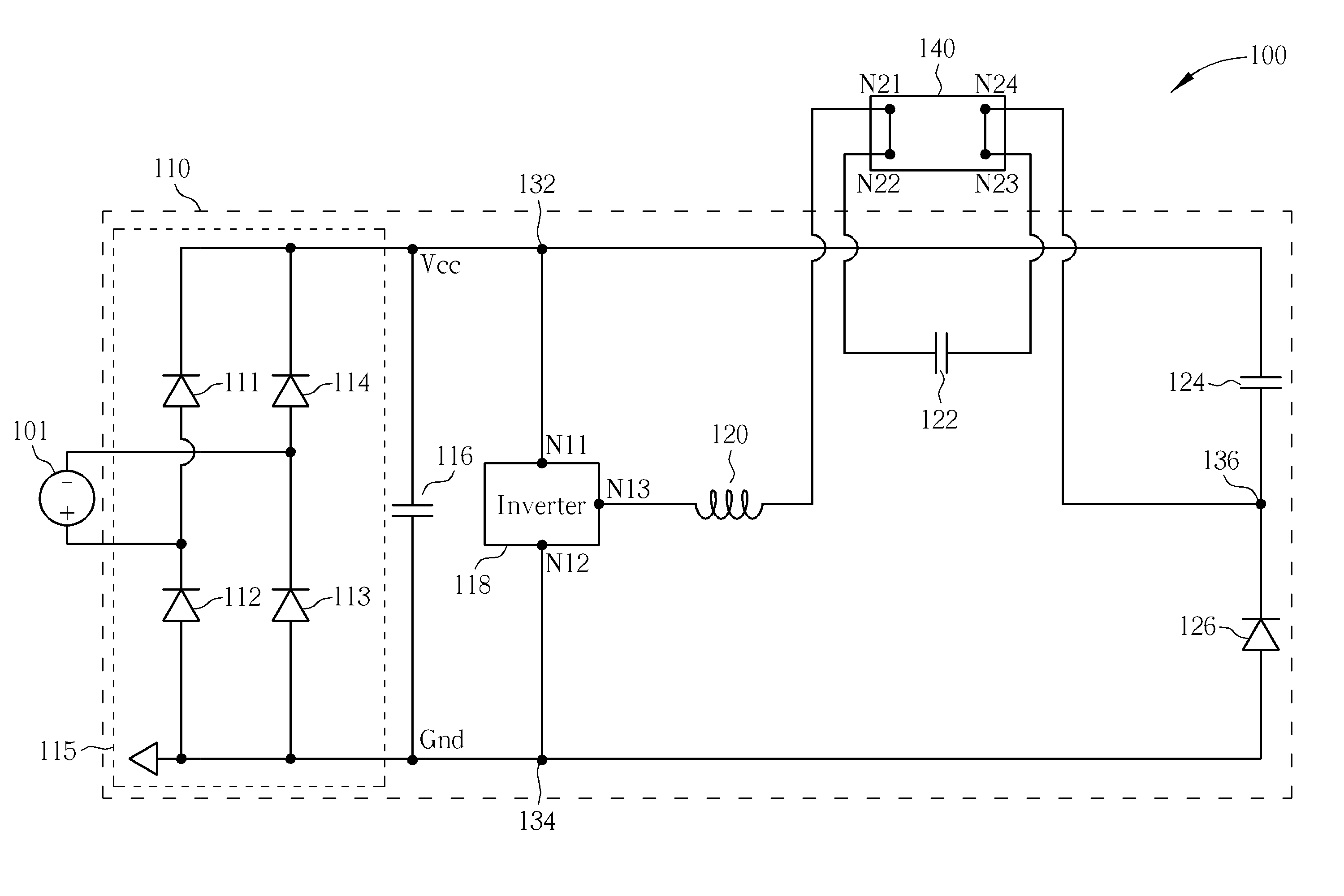
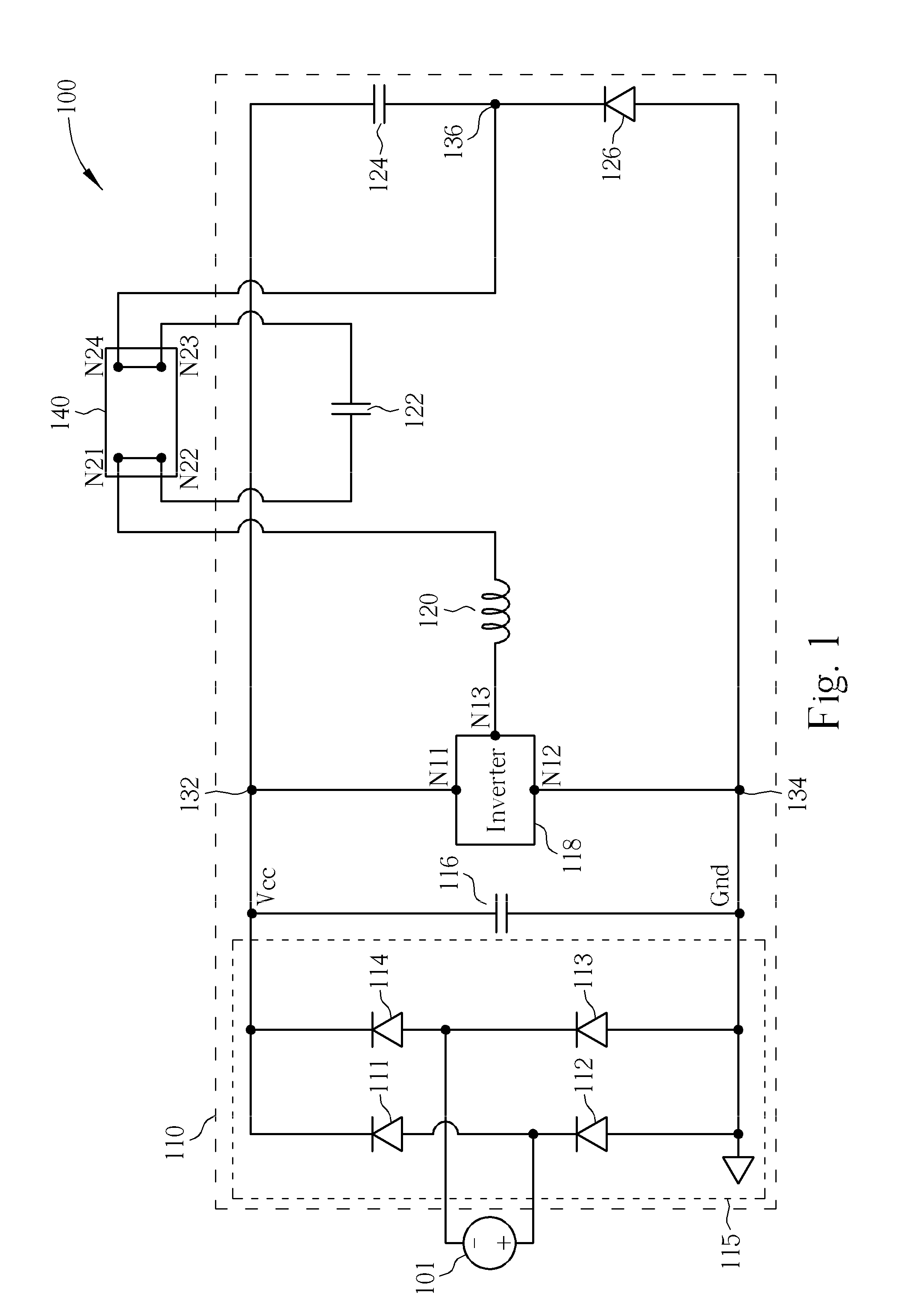
[0028]Please refer to FIG. 1, which is a circuit diagram schematically showing an electronic ballast in accordance with the present invention. As shown in FIG. 1, the lighting system 100 comprises an ac (alternating current) input source 101, an electronic ballast 110 and a lamp 140. The ac input source 101 is employed to generate an ac input voltage. In this embodiment, the lamp 140 is a compact fluorescent lamp (CFL), but this should not be construed as a limitation of the present invention. The electronic ballast 110 is coupled with the ac input source 101 and the lamp 140 for powering the lamp 140.
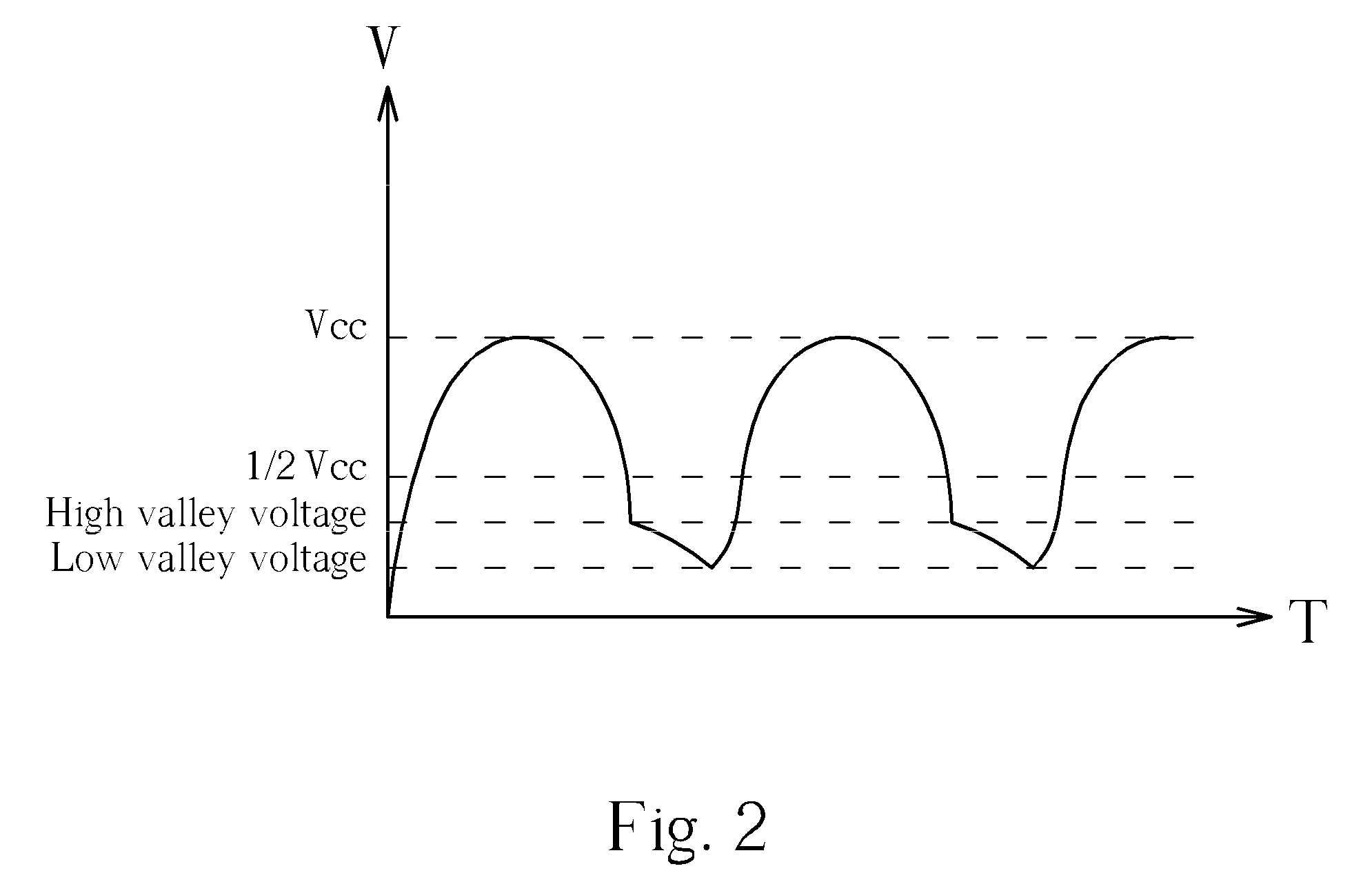
[0029]The electronic ballast 110 includes, but is not limited to, a rectifier circuit 115, a first capacitor 116, an inverter 118, a first inductor 120, a second capacitor 122, a third capacitor 124 and a diode 126. The rectifier circuit 115 functions to convert the ac input voltage into a dc (direct current) voltage (i.e., a mains voltage). A pair of input terminals of the rectifier c...
second embodiment
[0033]Please refer to FIG. 3, which is a circuit diagram schematically showing an electronic ballast in accordance with the present invention. As shown in FIG. 3, the lighting system 300 includes, but is not limited to, the ac input source 101, the lamp 140 and an electronic ballast 310. The electronic ballast 310 is similar to the electronic ballast 110 shown in FIG. 1, and the major difference there between is a fourth capacitor 328 and a second diode 330 included in the electronic ballast 310 in FIG. 3. The fourth capacitor 328 has a first end coupled to the first node 132 and a second end coupled to the fourth terminal N24 of the lamp 140. The fourth capacitor 328 is used for terminating the lamp 140 to the voltage Vcc to achieve dc isolation for the lamp 140. The second diode 330 has a cathode coupled to the second end of the fourth capacitor 328 and an anode coupled to the third node 136. The second diode 330 only allows one-way current to charge the third capacitor 124 and th...
third embodiment
[0035]Please refer to FIG. 4, which is a circuit diagram schematically showing an electronic ballast in accordance with the present invention. As shown in FIG. 4, the lighting system 400 includes, but is not limited to, the ac input source 101, the lamp 140 and an electronic ballast 410. The electronic ballast 410 is similar to the electronic ballast 310 shown in FIG. 3, and the major difference there between is a second inductor 432 included in the electronic ballast 410 in FIG. 4. The second inductor 432 has two ends coupled to the second end of the fourth capacitor 328 and the third terminal N13 of the inverter 118, respectively. The second inductor 432 is added to eliminate the dc voltage drop of the valley voltage due to the IR loss of the lamp 140. Because the dc current charging the third capacitor 124 will flow though the second inductor 432 instead of flowing through the first inductor 120 and the lamp 140, the IR loss of the lighting system 400 can be decreased greatly.
[00...
PUM
 Abstract
Description
Claims
Application Information
 - R&D Engineer
- R&D Manager
- IP Professional
- Industry Leading Data Capabilities
- Powerful AI technology
- Patent DNA Extraction
Browse by: Latest US Patents, China's latest patents, Technical Efficacy Thesaurus, Application Domain, Technology Topic, Popular Technical Reports.
© 2024 PatSnap. All rights reserved.Legal|Privacy policy|Modern Slavery Act Transparency Statement|Sitemap|About US| Contact US: help@patsnap.com


