
Photovoltaic Cell Module And Method Of Forming Same

a photovoltaic cell and module technology, applied in the field of photovoltaic cell modules, can solve the problems of low uv resistance of eva, low efficiency of encapsulation methods known in the art, and ineffective encapsulation methods, so as to improve durability and weatherability, reduce cost, and improve the effect of photovoltaic cell module production

Inactive Publication Date: 2011-03-17
DOW CORNING CORP
View PDF53 Cites 48 Cited by
  • Summary
  • Abstract
  • Description
  • Claims
  • Application Information

AI Technical Summary

Benefits of technology

The present invention is about a new photovoltaic cell module and method of making it that solves problems with current encapsulation methods. The module includes a substrate and a tie layer with specific properties that improve the performance and durability of the module. The method of making the module minimizes processing complexities and allows for the use of differing amounts of encapsulants to protect the electrical leads while maintaining performance. The technical effects of the invention are improved efficiency and durability of photovoltaic cell modules.

Problems solved by technology

However, encapsulants and encapsulation methods known in the art are expensive and time consuming and typically ineffective.
Hence, photovoltaic cells including EVA are limited to harvesting light at wavelengths above 400 nm.
More specifically, EVA has low UV resistance, has a tendency to discolor, and has a tendency to chemically and physically degrade upon exposure to light.
EVA is also known to exhibit poor adhesive properties relative to glass substrates and have a high modulus.
These poor adhesive properties and high modulus tend to cause high stress conditions around the photovoltaic cells resulting in gradual delamination of the encapsulant from the substrate.
This delamination leads to water accumulation in the encapsulant and photovoltaic cell corrosion.
However, this reduces a total amount of available light impinging on the photovoltaic cell, thereby reducing cell efficiency.
However, use of the doped glass or UV absorbers typically causes a 1% to 5% loss in photovoltaic cell efficiency.
Production of photovoltaic cells in this way is relatively expensive and time consuming.
This method tends to promote side reactions that reduce overall durability.
If peroxides are used, curing temperatures typically range from 150° C. to 160° C. These temperatures typically cause excessive stress in the photovoltaic cells and result in mechanical breakdown and / or increased production time and a number of steps needed to strengthen the photovoltaic cells.
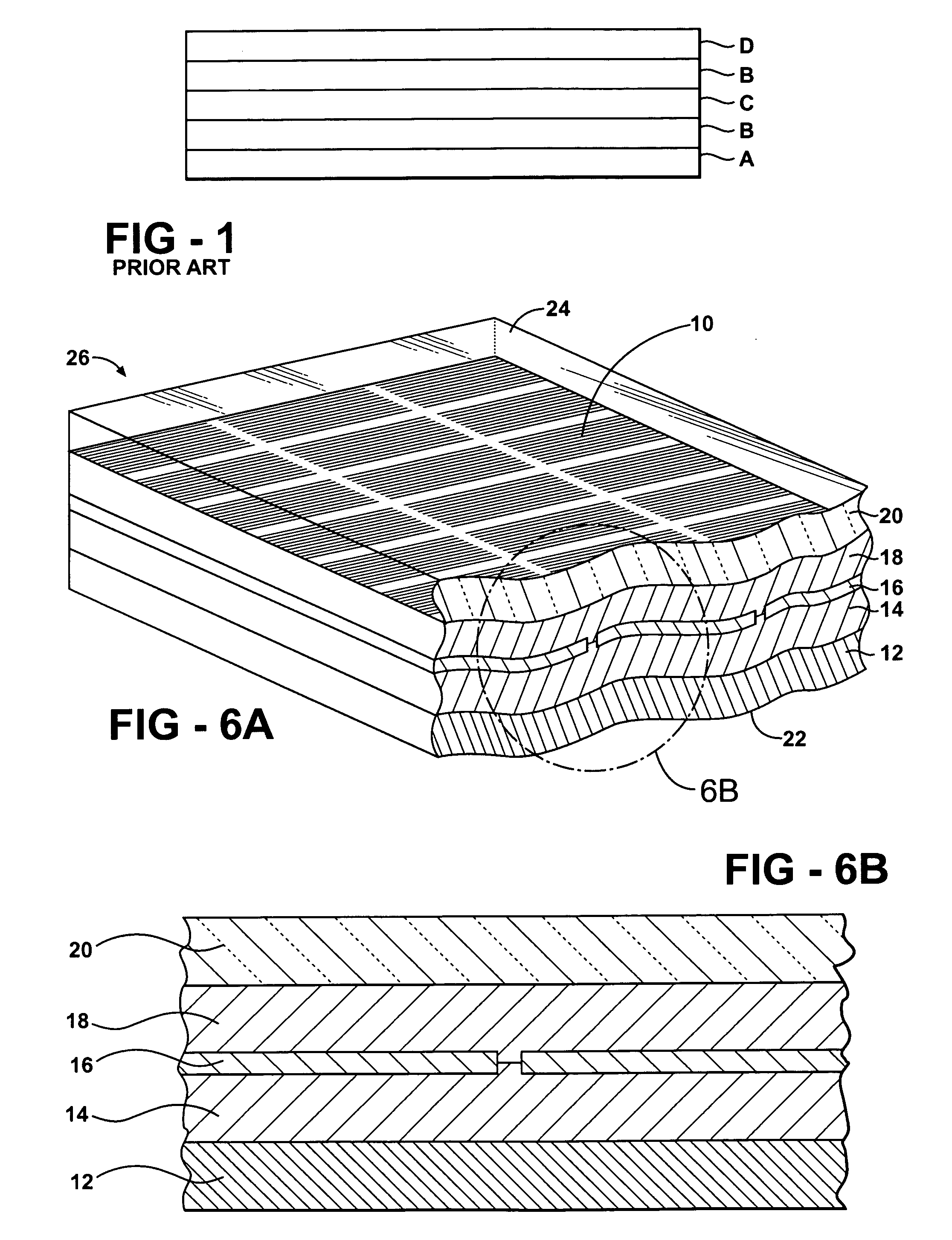
The glass superstrate (D), whilst transparent to light, is typically doped with cerium and antimony to filter UV light thereby increasing production costs and complexities.
In addition, silicones have been investigated for use as encapsulants but are not typically used due to numerous drawbacks resulting from production methods.
Whilst this method provides significant advantages over other encapsulation methods, the method tends to trap air bubbles underneath the photovoltaic cells which causes the photovoltaic cells to exhibit inferior properties.
Additional drawbacks include a difficulty in controlling thickness of the encapsulant, increased expense, increased processing times, and increased processing complexity.
These all result in increased cost for the end purchaser.
The prior art does not account for differing thicknesses of electrical leads that are included on photovoltaic cells in relation to detrimental exposure of such leads due to long term use of the photovoltaic cells, weathering, and general wear and tear.
The exposure of the leads results in decreased performance and decreased conversion of light into electricity.
Furthermore, the prior art does not account for the use of differing amounts of encapsulants to protect the electrical leads while maintaining performance and decreasing production costs.

Method used


Image

  • Photovoltaic Cell Module And Method Of Forming Same
  • Photovoltaic Cell Module And Method Of Forming Same
  • Photovoltaic Cell Module And Method Of Forming Same

Examples


examples

[0120]Two tie layers (Layers 1 and 2) are formed according to the instant invention. In addition, two comparative tie layers (Comparative Layers 1 and 2) are also formed but not according to the instant invention. During and after formation, each of the Layers 1 and 2 and the Comparative Layers 1 and 2 are evaluated to determine viscosity, Shore 00 durometer hardness, hardness, depth of penetration, and tack value. The formulations used to form Layers 1 and 2 and the Comparative Layers 1 and 2, in addition to the measurements of viscosity, Shore 00 durometer hardness, hardness, depth of penetration, and tack value are set forth in Table 1 below wherein all parts are in parts by weight, unless otherwise indicated.

TABLE 1ComparativeComparativeLayer 1Layer 2Layer 1Layer 2FormulationPolymer 198.9848.8135.180.49Polymer 2—41.87——Polymer 3———11.04Polymer 4—4.06—7.73Polymer 50.90.131.440.49Polymer 6—5.38——Cure0.040.010.190.17InhibitorCatalyst 10.08—0.09—Catalyst 2—0.14—0.08Filler——55.38—Pig...


PUM

PropertyMeasurementUnit
depth of penetrationaaaaaaaaaa
thicknessaaaaaaaaaa
thicknessaaaaaaaaaa

Abstract

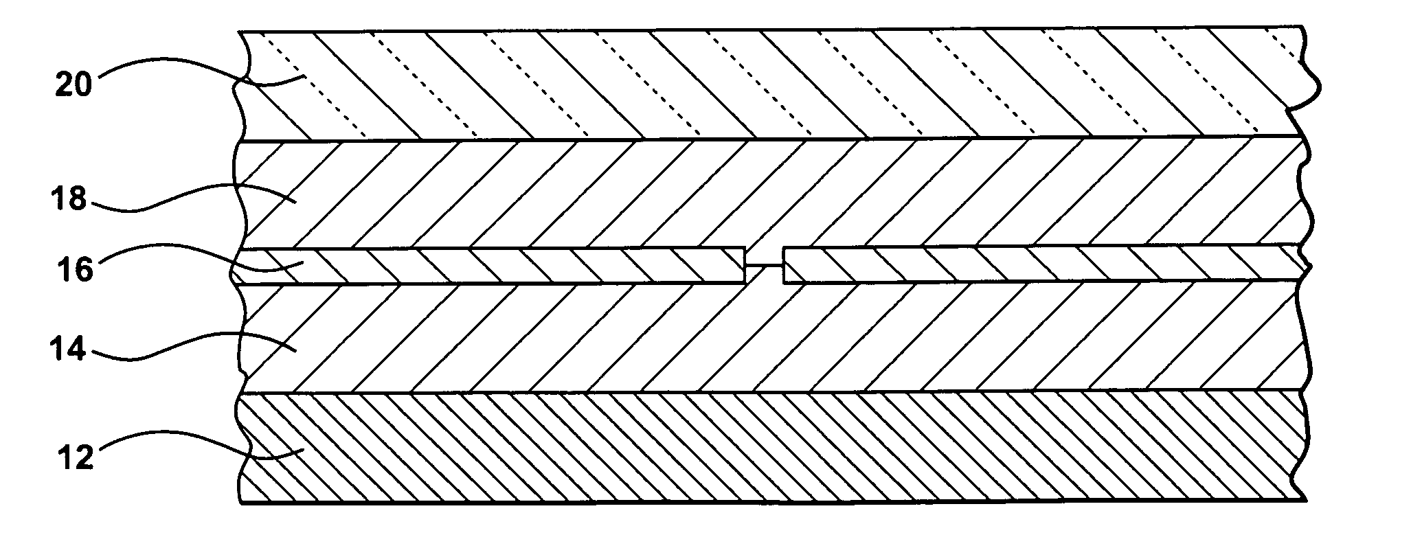
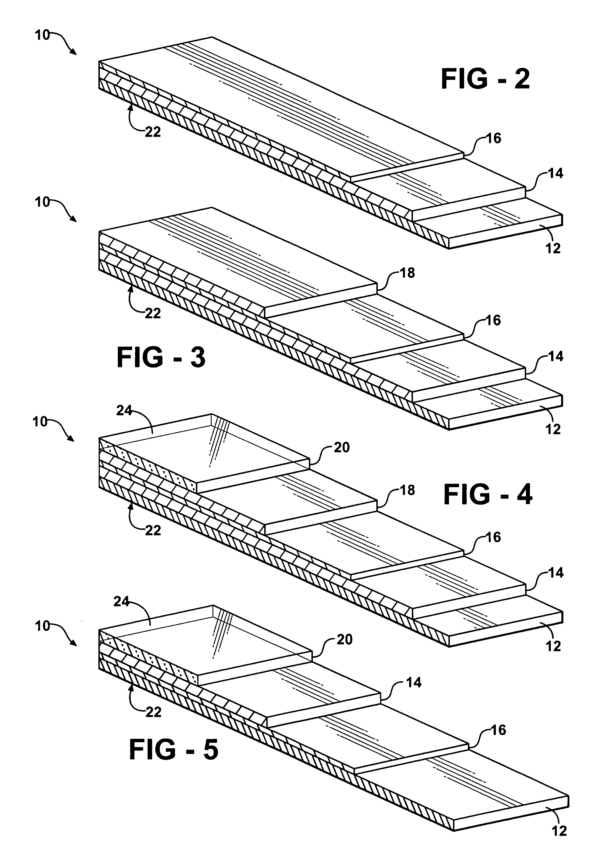
A photovoltaic cell module, a photovoltaic array including at least two modules, and a method of forming the module are provided. The photovoltaic cell module includes a substrate and a tie layer disposed on the substrate. The tie layer has a depth of penetration of from 1.1 to 100 mm and a tack value of less than −0.6 g·sec. The photovoltaic cell module also includes a photovoltaic cell disposed on the tie layer. The method of forming the photovoltaic cell module includes the steps of disposing the tie layer on the substrate and disposing the photovoltaic cell on the tie layer to form the photovoltaic cell module.

Description

CROSS-REFERENCE TO RELATED APPLICATIONS[0001]The subject patent application claims priority to, and all the benefits of, U.S. Provisional Patent Application Ser. Nos. 61 / 036,748 and 61 / 036,752, both filed on Mar. 14, 2008, and U.S. Provisional Patent Application Ser. No. 61 / 146,551 filed on Jan. 22, 2009. The entirety of these provisional patent applications is expressly incorporated herein by reference.FIELD OF THE INVENTION[0002]The present invention generally relates to a photovoltaic cell module and method of forming the same. More specifically, the photovoltaic cell module includes a substrate and a tie layer having particular properties that is disposed on the substrate.DESCRIPTION OF THE RELATED ART[0003]Solar or photovoltaic cells are semiconductor devices used to convert light into electricity. There are two general types of photovoltaic cells, wafers and thin films. Wafers are thin sheets of semiconductor material that are typically formed from casting or mechanically sawi...

Claims


Application Information

Patent Timeline
Patent Type & Authority Applications(United States)
IPC IPC(8): H01L31/048C23C14/34H01L31/18
CPCB32B37/003B32B37/10B32B37/1009B32B38/1858B32B2309/62B32B2309/68Y10T29/49115H01L21/67092H01L31/048H01L31/18Y02E10/50Y10T29/49108B32B2457/12H01L31/1876Y02P20/582Y02P70/50
Inventor HOULE, KEVINHOWELL, MALINDAJOHNSON, DAVIDJUEN, DONNIEKETOLA, BARRYSHEPHARD, NICK EVAN
Owner DOW CORNING CORP
Learn More