Printed circuit board and method of manufacturing the same

Inactive Publication Date: 2011-03-17
SAMSUNG ELECTRO MECHANICS CO LTD
View PDF13 Cites 14 Cited by
  • Summary
  • Abstract
  • Description
  • Claims
  • Application Information

AI Technical Summary

Benefits of technology

[0012]An aspect of the present invention provides a printed circuit board and a method of manufacturing the same capable of impr

Problems solved by technology

The bending of the semiconductor package board markedly affects the manufacturing rate and productivity thereof in implementing such a soldering process.
In addition, the bending of the semiconductor package board may cause a problem in which a solder ball is not formed on a solder ball pad of the semiconductor package board in a soldering process, a problem in which solder balls formed on a semiconductor element and the semiconductor package board are not bonded to each other in the process of mounting the semiconductor element, or the like, depending on the degree of bending.
Accordingly, the bending of the semiconductor packag

Method used


Image

  • Printed circuit board and method of manufacturing the same
  • Printed circuit board and method of manufacturing the same
  • Printed circuit board and method of manufacturing the same

Examples


first embodiment

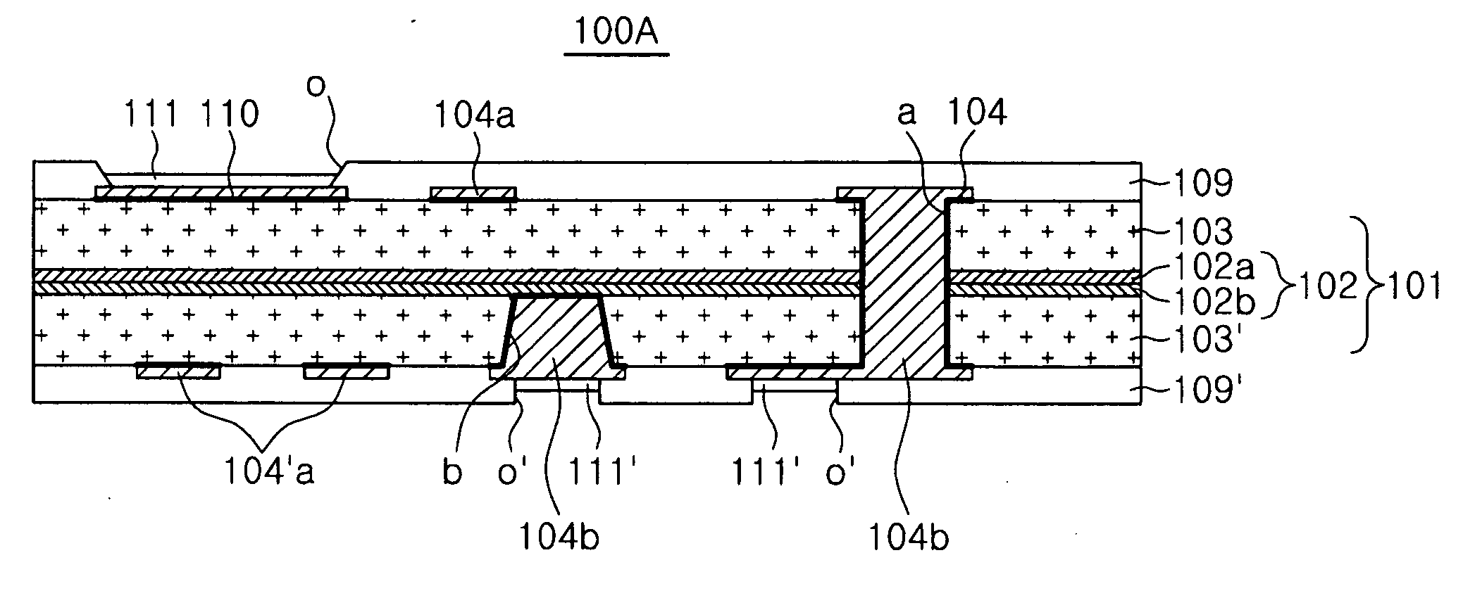
[0035]FIGS. 1A and 1B are schematic cross-sectional views of a printed circuit board including a bending prevention portion according to an exemplary embodiment of the present invention. The printed circuit board will be described based on a two-layered printed circuit board having a bending prevention portion as an example.

[0036]The printed circuit board 100A according to the exemplary embodiment of the present invention is configured to include a core layer 101 that includes a bending prevention portion 102 interposed between insulating members 103 and 103′ and insulating layers 109 and 109′ that are formed on circuit patterns 104 and 104′, which are in turn formed on the inner side of the core layer 101 or the outer side of the insulating members 103 and 103′, and the insulating members 103 and 103′ and include opening portions O and O′ that expose the circuit patterns 104 and 104′ so as to be bonded to solder balls.

[0037]Here, the bending prevention portion 102 is interposed be...

second embodiment

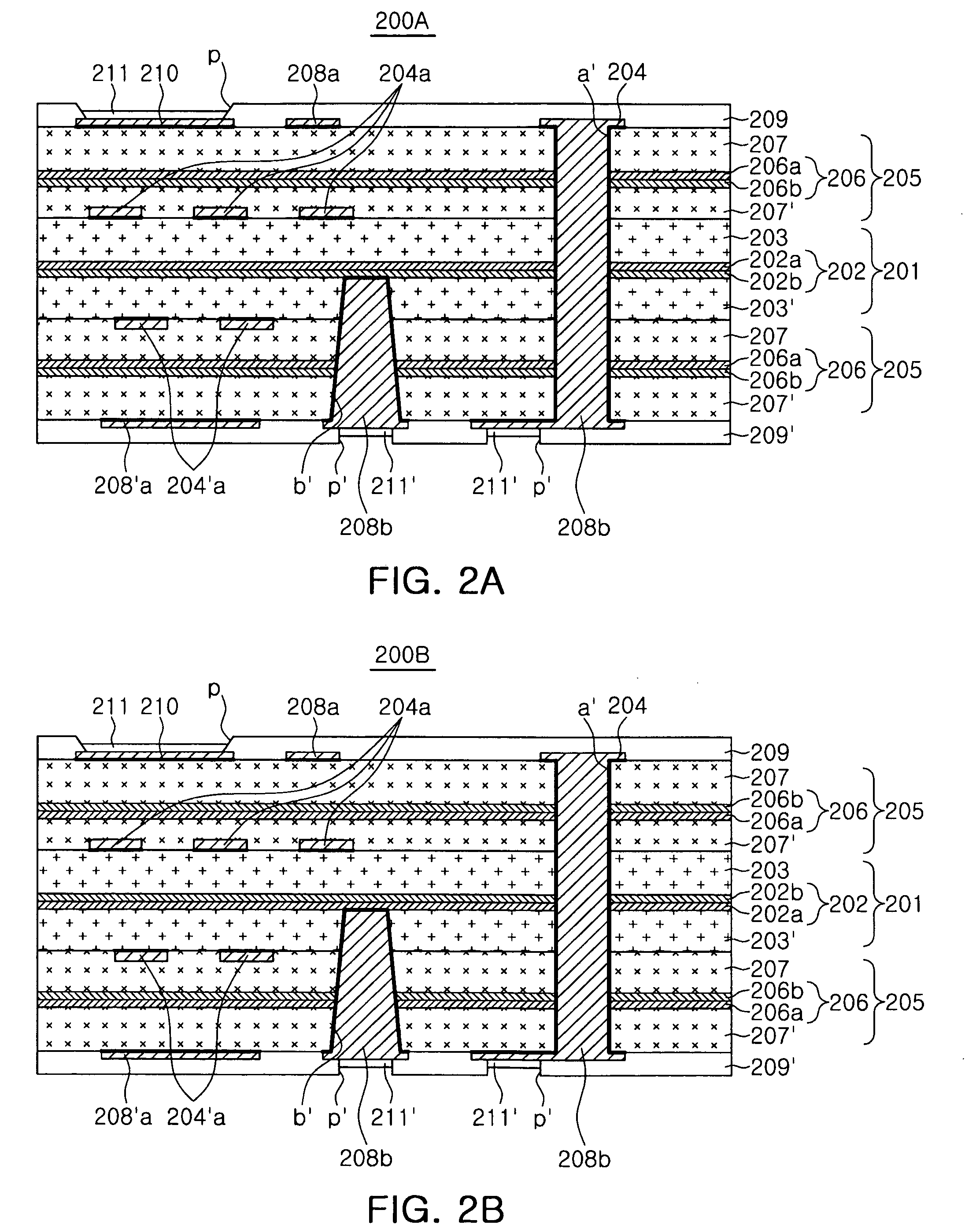
[0047]The printed circuit board 200A according to the present invention is configured to include: a core layer 201 that includes a bending prevention portion 202 interposed between insulating members 203 and 203′; core layers 205 that are formed on circuit patterns 204 and 204′, in turn formed on the inner side of the core layer 201 or the outer side of the insulating members 203 and 203′, and the insulating members 203 and 203′; and a solder resist 209 that is patterned so as to expose the circuit patterns 208 and 208′ of the core layer 205.

[0048]Here, the bending prevention portion 202 is interposed between the insulating members 203 and 203′. The bending prevention portion 202 is configured by two-layer metals having different thermal expansion coefficients and is disposed in the core layer 201.

[0049]In a case where the printed circuit board 200A is used as an upper board of a POP (Package On Package) board, the bending prevention portion 202 is configured to include a first bend...


PUM

PropertyMeasurementUnit
Bending strengthaaaaaaaaaa
Thermal expansion coefficientaaaaaaaaaa

Abstract

There is provided a printed circuit board. The printed circuit board may be configured to include: a core layer in which a bending prevention portion of at least two layers is interposed between a plurality of insulating members and includes metal layers having different thermal expansion coefficients is disposed; a circuit pattern that is formed so as to have a desired pattern on at least one of the inside of the core layer and an outer face of the core layer; and an insulating layer that is formed on the core layer and includes an opening portion that exposes the circuit pattern, and a method of manufacturing the printed circuit board. According to the above-described printed circuit board and the method of manufacturing the printed circuit board, by disposing a bending prevention portion inside the printed circuit board, a printed circuit board capable of improving the progress rate and the productivity and a method of manufacturing the printed circuit board can be provided.

Description

CROSS-REFERENCE TO RELATED APPLICATIONS[0001]This application claims the priority of Korean Patent Application No. 10-2009-0087152 filed on Sep. 15, 2009, in the Korean Intellectual Property Office, the disclosure of which is incorporated herein by reference.BACKGROUND OF THE INVENTION[0002]1. Field of the Invention[0003]The present invention relates to a printed circuit board and a method of manufacturing thereof, and more particularly, to a printed circuit board capable of improving a manufacturing rate and productivity thereof by disposing a bending prevention portion inside the printed circuit board and a method of manufacturing the same.[0004]2. Description of the Related Art[0005]Recently, companies assembling and manufacturing circuit boards are focused on super precision technology in accordance with the trend of semiconductor package boards towards lightness, thinness, and compactness.[0006]In particular, in a soldering process in which electrical bonding is connected betwe...

Claims


Application Information

Patent Timeline
IPC IPC(8): H05K1/03H05K3/36
CPCY10T29/49165H05K1/09H05K2201/0352H05K2201/068Y10T29/49128H05K3/10Y10T428/24917H05K2201/0338Y10T29/49124H05K1/0271H05K3/4602Y10T29/49126H05K2201/09136H05K1/03
Inventor HWANG, MI SUNLEE, JAE JOONKANG, MYUNG SAM
Owner SAMSUNG ELECTRO MECHANICS CO LTD
Why Eureka
Try Eureka