Flexible substrate and method for fabricating flexible display devicve having the same

US20110062444A1Active Publication Date: 2011-03-17LG DISPLAY CO LTD

Image

  • Flexible substrate and method for fabricating flexible display devicve having the same
  • Flexible substrate and method for fabricating flexible display devicve having the same
  • Flexible substrate and method for fabricating flexible display devicve having the same

Examples


Embodiment Construction

[0025]Reference will now be made in detail to the embodiments of the present invention, examples of which are illustrated in the accompanying drawings.

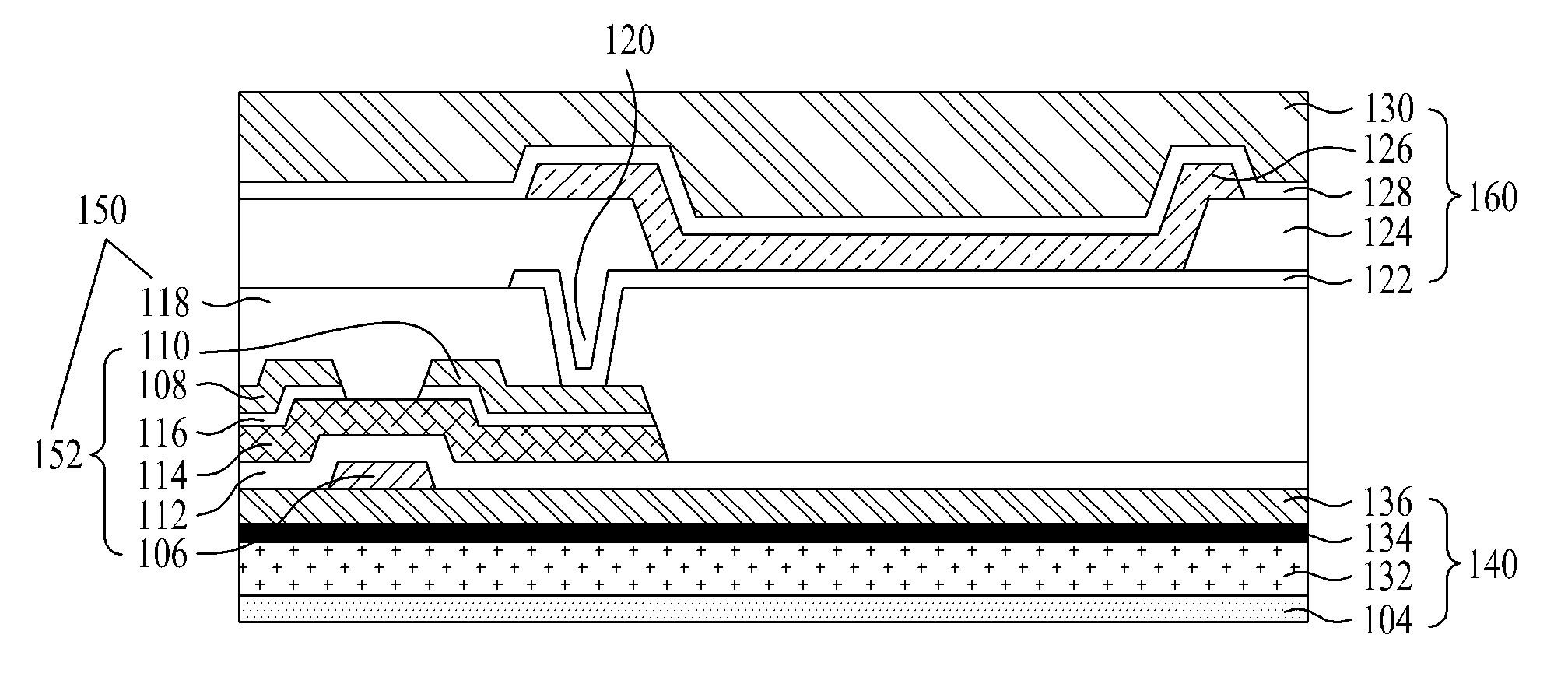
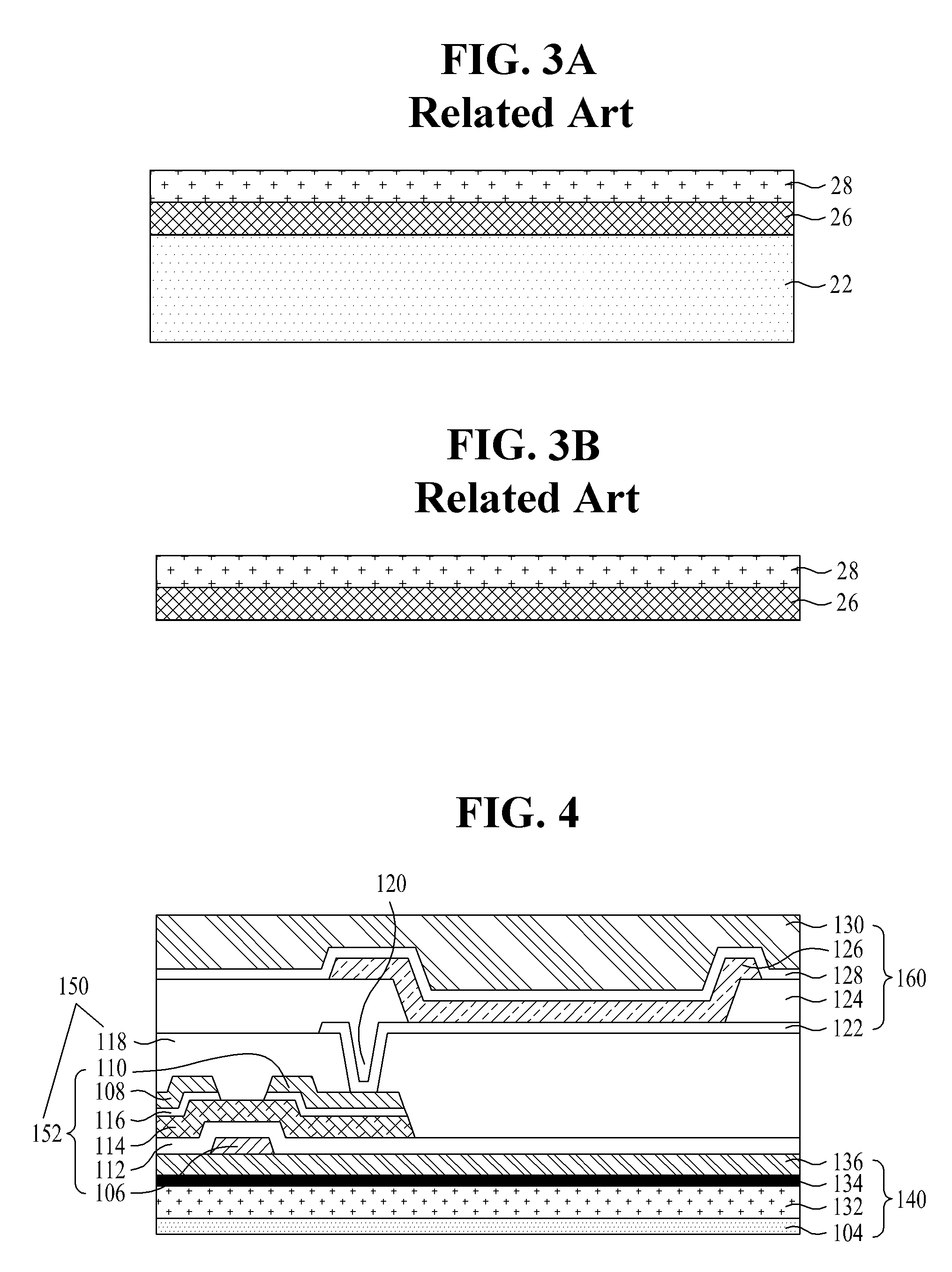
[0026]FIG. 4 is a cross-sectional view illustrating an exemplary organic electroluminescence display device having a flexible substrate in accordance with the present invention. The present invention will be described taking an organic electroluminescence display device as an example, but is not limited thereto.

[0027]With reference to FIG. 4, the organic electroluminescence display device includes a flexible substrate 140, a thin film transistor array 150, and an organic electroluminescence array 160. The flexible substrate 140 includes a semiconductor layer 104, a first flexible layer 132, an adhesive 134, and a second flexible layer 136. The organic electroluminescence array 160 includes a cathode electrode 122, a bank insulating film 124, an organic electroluminescence layer 126, an anode electrode 128, and a sealing member 130.

[00...


PUM


Abstract

A method for fabricating a flexible display device including the steps of preparing a glass substrate, forming a flexible substrate on the glass substrate, the flexible substrate being formed by forming a semiconductor layer on the glass substrate, forming a first flexible layer on the semiconductor layer, forming an adhesive layer on the first flexible layer, and forming a second flexible layer on the adhesive layer, forming a thin film array on the flexible substrate, forming a display device on the thin film array, and separating the glass substrate from the semiconductor layer of the flexible substrate.

Description

[0001]This application claims the benefit of the Korean Patent Application No. 10-2009-0087656, filed on Sep. 16, 2009, which is hereby incorporated by reference.BACKGROUND OF THE INVENTION[0002]1. Field of the Invention[0003]The present invention relates to flat panel display devices, and more particularly, to a flexible substrate which simplifies a fabrication process and prevents deformation, and a method for fabricating a flexible display device having the same.[0004]2. Discussion of the Related Art[0005]Currently, display device markets have become markets of flat display devices. Also, increased use of flat display devices has allow for easier fabrication of large size and light weight devices. Flat display devices include liquid crystal display devices LCD, plasma display panel PDP, organic electroluminescence display device OLED, and the like. Flat display devices use glass substrates as supporting bodies for supporting a plurality of thin films. However, there are problems ...

Claims


Application Information

Patent Timeline
17 Mar 2011
Publication
US20110062444A1
IPC
H01L33/16; H01L21/77
CPC
H01L27/1266; G02F1/136; G02F1/1333
Inventors
PARK, DONG SIK; YOO, JUHN-SUK