Optical phase modulator and optical phase modulating device

a technology of optical phase modulator and optical phase, which is applied in the direction of optics, optical elements, instruments, etc., can solve the problems of small light loss of mz modulator that uses linbo3 and high driving voltage, and achieve the effect of reducing the effect of frequency chirping

Active Publication Date: 2011-03-17
FURUKAWA ELECTRIC CO LTD
View PDF28 Cites 17 Cited by
  • Summary
  • Abstract
  • Description
  • Claims
  • Application Information

AI Technical Summary

Benefits of technology

[0024]With the present invention it is possible to provide an optical phase modulator and optical phase modulating device that are capable of reducing the effects of frequency chirping caused by an orthogonal component that occurs due to light absorption by a semiconductor.

Problems solved by technology

A MZ modulator that uses LiNbO3 is characterized by having small light loss, however, the size is several inches, which is large, and the driving voltage is also high.

Method used


Image

  • Optical phase modulator and optical phase modulating device
  • Optical phase modulator and optical phase modulating device
  • Optical phase modulator and optical phase modulating device

Examples


embodiment 1

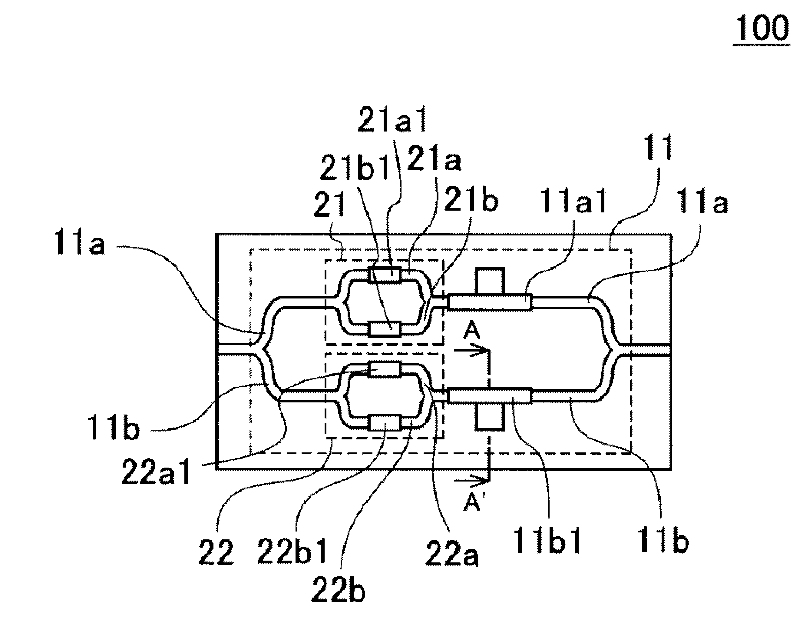
[0047]The construction of an optical phase modulation of a first embodiment of the present invention will be explained using FIG. 1. FIG. 1 is a top view that schematically illustrates the construction of a DPSK optical phase modulator as one example of binary optical phase modulators, which is the optical phase modulator of a first embodiment of the present invention. The DPSK optical phase modulator 100 is formed on a semiconductor substrate and the optical waveguide paths are formed using semiconductor layers. The DPSK optical phase modulator 100 comprises a Mach-Zehnder interferometer 11 having two main optical waveguide path arms 11a, 11b, with a first high-frequency electrode 11a1 and second high-frequency electrode 11b1 being provided in the main optical waveguide path arms 11a, 11b, respectively. In addition, a sub Mach-Zehnder interferometer 21 comprising a first sub optical waveguide path arm 21a and a second sub optical waveguide path arm 21b is provided in the main optic...

embodiment 2

[0098]FIG. 13 will be used to explain the construction of an optical phase modulator of a second embodiment of the present invention. FIG. 13 is a top view that schematically illustrates the construction of a DQPSK optical phase modulator as one example of 4-value optical phase modulators of a second embodiment of the invention. As illustrated in FIG. 13, the DQPSK optical phase modulator 300 is such that two of the DPSK optical phase modulators 200 explained as a variation of the first embodiment (200-1, 200-2) are connected in parallel using a branching optical waveguide path 31 and combining optical waveguide path 32, where a phase shifter 30 that shifts the phase of the passing light by just π / 2 is provided in one of the branches of the branching optical waveguide path 31. The phase shifter 30 could also be provided in one of the branches of the combining optical waveguide path 32.

[0099]Of the DQPSK optical phase modulator 300, the area 2, in which first through sixth high-frequ...

embodiment 3

[0105]The optical phase modulator or optical phase modulating device of the present invention can be universally applied as described below to a higher-degree of multi-value optical modulators than the 4-value phase modulator (DQPSK) explained for the second embodiment.

[0106]In other words, two branch dividers can be connected in an n-level cascade connection (where n is a natural number) to form a branching optical waveguide path having 2n number of branch ends, where 2n number of 2-value optical phase modulators or 2-value optical phase modulating devices are connected in parallel to the 2n number of branch ends. In addition, a combining optical waveguide path comprising two-branch combining units that are connected in an n-level cascade connection is connected to the output ends of the 2n number of 2-value optical phase modulators or 2-value optical phase modulating devices to combine the output light from all of the 2-value optical phase modulators or 2-value optical phase modul...


PUM

PropertyMeasurementUnit
thicknessaaaaaaaaaa
phaseaaaaaaaaaa
phase differenceaaaaaaaaaa

Abstract

The optical phase modulator of the present invention comprises: a main Mach-Zehnder interferometer having first and second main optical waveguide path arms, and whose initial phase difference in the used wavelength is π; a first sub Mach-Zehnder interferometer having first and second sub optical waveguide path arms that are formed in said first main optical waveguide path arm, and whose initial phase difference in the used wavelength is 0; and a second sub Mach-Zehnder interferometer having third and fourth sub optical waveguide path arms that are formed in said second main optical waveguide path arm, and whose initial phase difference in the used wavelength is 0. Of each of the main optical waveguide path arms and first through fourth sub optical waveguide path arms, at least the portions where high-frequency electrodes are formed is constructed using semiconductor waveguide paths, and are capable of reducing the effects of frequency chirping caused by an orthogonal component that occurs due to light absorption in the semiconductor.

Description

CROSS-REFERENCE TO RELATED APPLICATIONS[0001]This application claims priority from Japanese patent application No. 2009-167703, filed on Jul. 16, 2009, the entire content of which is incorporated herein by reference.BACKGROUND OF THE INVENTION[0002]1. Field of the Invention[0003]The present invention relates to an optical phase modulator and optical phase modulating device that are used in optical phase modulating using optical phase.[0004]2. Description of the Related Art[0005]In addition to conventional intensity modulation as a method of modulating light in optical communication by an electrical signal, there is also optical phase modulation. Optical phase modulation differs from conventional optical intensity modulation, which performs modulation between ON and OFF of the optical intensity; for example, the followings are known, i.e., there is binary optical phase modulation (for example, DPSK: Differential Phase Shift Keying) that performs modulation using two different optical...

Claims


Application Information

Patent Timeline
Patent Type & Authority Applications(United States)
IPC IPC(8): G02F1/035
CPCG02F1/0121G02F2001/212G02F1/2257G02F1/2255H04B10/50575G02F1/212
Inventor KISE, TOMOFUMIFUNABSHI, MASAKI
Owner FURUKAWA ELECTRIC CO LTD
Why Eureka
Try Eureka