Broad spectrum light source calibration systems and related methods
Active Publication Date: 2011-03-24
LUTRON TECH CO LLC
58 Cites 99 Cited by
AI-Extracted Technical Summary
Problems solved by technology
Since there are infinitely more colors not on the black body curve than on the black body curve and since phosphor thickness and emission spectrums cannot be precisely controlled, it is very difficult to produce white LEDs with a specific and defined color temperature.
Since the phosphor coating in most white LEDs convert high energy blue photons into lower energy photons in the green, yellow, and red range, the phosphor absorbs energy which reduces the optical efficiency of the LED and produces heat, both of which are not desirable.
Although combining white and red LEDs to produce warmer color temperatures or more red spectral content improves performance parameters including energy efficiency and heat dissipation, controlling the color point is more difficult since the brightness of the red LEDs change differently with temperature, time, and other operating conditions than the white LEDs.
Not only do the extra components add cost, but since the light sensor is only sensitive to the shorter (bluer) wavelengths produced ...
View moreBenefits of technology
[0020]The calibration methods and apparatus described herein address issues for devices using groups of different colored LEDs directly or as backlights for illumination. Such calibration methods re...
View moreAbstract
Systems and methods are disclosed for light sources that use the photo-sensitivity of one or more colored LEDs to determine at least a portion of the emission spectrum of a white light source or other broad spectrum light emitter. As described herein, a white LED or other broad spectrum light emitter can be used as the light source, if desired, along with one or more additional colored LEDs, and the same colored LEDs can be used to emit light and to adjust a color point produced by the light source. Applications for the disclosed embodiments include but are not limited to general lighting, LCD backlighting, projectors, and direct emission displays such as OLEDs and digital billboards.
Application Domain
Technology Topic
Image
Examples
- Experimental program(8)
Example
First Embodiment
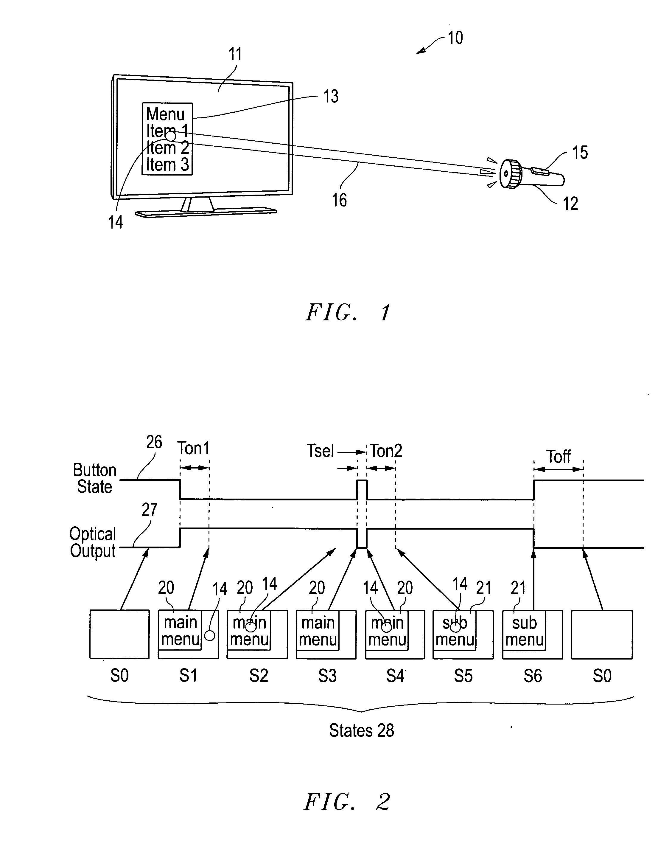
[0117]Display and optical pointer systems and related methods are disclosed that utilize LEDs in a display device to respond to optical signals from optical pointing devices. Various embodiments are described with respect to the drawings below. Other features and variations can also be implemented, if desired, and related systems and methods can be utilized, as well.
[0118]In part, the disclosed embodiments relate to displays with arrays of LEDs and associated pointing devices that communicate with individual LEDs in the arrays using visible light. The LED arrays can produce images directly as in LED billboards and sports arena scoreboards or can produce the backlight for LCD screens for instance. The pointing devices communicate with individual pixels or groups of pixels using a beam of light that may or may not be modulated with data, which is detected by the LEDs in the array that are exposed to the beam. Periodically, the LEDs in an array stop producing light and are configured with an associated driver device to detect light from the pointing device. Such a configuration enables the user to point and click at on screen displays much like a computer mouse.
[0119]One improved system, as described herein, uses an optical pointing device, such as a laser pointer or flashlight, to control a graphical user interface for instance, on an LCD display with LED backlights or a display made from an array of organic or conventional LEDs. As an image is scanned across such a display, there are times every frame when the LEDs are not producing light. During such light off times, the LEDs are used to detect the presence or absence of light from the optical pointing device. The graphics controller processes such information over a series of frames to detect a pattern of light from the pointing device illuminating a particular location on the display and takes the appropriate action. Such action could be among other things selecting an item in a menu, dragging and dropping an item, or popping up a menu.
[0120]The simplest pointing device could be a laser pointer or flashlight with a single on/off button. With a display playing a video or a television broadcast for instance, the display could pop up a main menu over part of the screen in response to a bright spot of light detected anywhere on the display. Once the spot is positioned over a particular item in the menu, such as change channel for a television, and then turned off and on again, the appropriate action could be taken. With a display, such as a billboard, advertising merchandise for instance, patterns of light on and off from a pointing device could cause the display to provide more information about a particular item. These are just some examples of interactions between a display and a pointing device, with many more possible.
[0121]With more sophisticated pointing devices and displays, data could be communicated from the pointing device to the display and potentially even from the display to pointing device. For instance, a laser pointer specially modified to produce light modulated with data could transmit personal information, such as an email address, to a display, such as a billboard. A user could instruct the display to send more information to an email address in this example. Again, this example is just one of many possible data communication applications.
[0122]The types of displays addressed herein include any that use LEDs for illumination, but typically can be divided into three categories, Organic LED (OLED) displays, conventional LED displays, and liquid crystal displays (LCDs) with LED backlighting. OLED displays typically comprise a piece of glass with thin film transistors and LEDs made from organic compounds grown on one side to produce an array of pixels typically comprising red, green, blue, and white sub-pixels. Each sub-pixel typically has a current source made from the thin film transistors that is controlled by column and row drivers typically situated on two sides of the perimeter of the glass. The row drivers typically produce a logic level write signal to a row of pixels or sub-pixels while the column drivers produce an analog voltage corresponding to the desired sub-pixel current. Such voltage is typically stored on a capacitor in each pixel or sub-pixel.
[0123]Video images are typically displayed one row at a time as the row drivers sequence the write signals to the OLED array typically from the top to bottom of the array. Moving images are produced a series of still images or frames displayed over time. As one image is displayed one row at a time, the previous image is removed one row at a time. To prevent the well known visual effect called “motion blur”. Every row of LEDs is turned off for a period of time, which removes the previous frame, before displaying a line of the current frame. A high speed snapshot of an OLED display properly designed to reduce motion blur will show a band of LED rows illuminated with the rest of the display is dark. The row drivers typically write to each row of pixels or sub-pixels twice per frame in order to turn the LEDs on and then off.
[0124]The spot on the display illuminated by the pointing device is detected one row at a time. According to one embodiment, the row drivers produce sense signals sequentially to each pixel or sub-pixel row at some offset from the rows producing light to prevent optical crosstalk from the rows producing light to the row detecting light. When a sense signal is active, each sub-pixel in the row can produce a current if the voltage induced across the associated LED by incident light is greater than a certain level, which can then be detected across the columns by current sense circuitry associated with the column drivers. The graphics controller monitors the current sense circuitry output for each row over a frame to determine the location of the illumination from the pointing device, and over many frames to determine the action to take.
[0125]Although OLED pixels typically comprise a number of different colored LEDs, such as red, green, blue, and white, typically only one color is used to detect the illumination from the pointing device. For instance, if a red laser pointer is used as the pointing device, the red sub-pixels in the display are used to detect the illumination. If a flashlight producing white light is the pointing device, the red or green sub-pixels in the display may be used to detect the illumination depending on the spectrum of the white light.
[0126]Displays made from conventional LEDs, which typically comprise of the element Gallium and are individually packaged, typically are very large and are used for billboards or video displays in sports stadiums. As with small OLED displays, each pixel typically comprises red, green, and blue sub-pixels, but typically do not have white sub-pixels. Each sub-pixel LED typically is driven by a current source from an LED driver IC (integrated circuit), which typically comprises a number of current sources associated with a number of sub-pixels. Such ICs can be serially connected together and through a network interface IC to a graphics controller, which produces the pixel data, receives the location of the illumination from the pointing device, and takes the appropriate action.
[0127]Each driver IC comprises a current source controlled by a pulse width modulator to produce light from each associated LED, and a comparator to detect light incident on each LED. Unlike the OLED display, each LED is driven with a fixed current for a variable amount time, instead of a variable current for fixed amount of time. The pulse width modulator associated with each LED receives a digital value from the graphics controller each frame and turns on the associated current source for a proportional amount of time. The maximum digital value corresponds to a maximum amount of time the current source can be on, which should be less than a frame period to prevent motion blur.
[0128]During the time between frames when the current source associated with a particular LED is guaranteed to be off, the illumination from the pointing device can be detected. If the voltage induced across the LED by incident light is greater than a certain value, the associated comparator output goes high indicating the presence of light from the pointing device. If the induced voltage is less than the certain amount, the comparator output is low indicating the absence of light. The state of all the comparator outputs is communicated back to the graphics controller for processing.
[0129]Like the OLED display, a conventional LED display is typically scanned one row or column at a time, which at any one time produces a band of illuminated LEDs across the display. The rest of the display is dark. To prevent optical crosstalk from LEDs producing light to LEDs detecting light, each LED driver IC typically samples the comparator outputs when the associated LEDs are located near the middle of the dark region.
[0130]Liquid crystal displays modulate the amount of light produced by a backlight to create an image on the screen. Backlights comprising LEDs typically come in one of two versions. For smaller displays on a laptop computer for instance, LEDs situated along one side of the display inject light into a diffuser that produces uniform white light across the display. For large screen televisions using LED backlights, the LEDs are typically arranged in an array, like the conventional LED display, behind the liquid crystal pixel array. The amount of light produced by each LED or group of LEDs can be adjusted per frame to increase the contrast ratio in a manner called “local dimming”, which not possible for LCDs with fluorescent backlights or LED backlights situated along one side of the display.
[0131]LED backlights for LCDs typically comprise of either white LEDs, which are made from blue LEDs with a yellow phosphor coating, or a combination of red, green, and blue LEDs, for instance. One embodiment uses colored LEDs configured in an array, like a conventional LED display, for LCD backlighting.
[0132]A liquid crystal pixel array typically comprises a thin film transistor and capacitor associated with each liquid crystal sub-pixel. The transparency of the liquid crystal sub-pixel is determined by the voltage held on the capacitor and is controlled by the associated row and column drivers. Like the OLED display, the liquid crystal array is typically written one row at a time when the associated logic level write signal goes active. The analog voltages from the column drivers are then transferred on to the capacitors through the transistors in each pixel element in the row. Typically, this analog voltage is held for one frame period, until that row is programmed with data for the next frame.
[0133]To reduce motion blur, the backlight array can be scanned so that the display only produces light from any given row for a portion of a frame period. A band of light produced by the LED backlight array follows the updating of the liquid crystal rows by a fixed offset to allow the liquid crystal element time to settle. The LEDs in the backlight array can be connected to the same driver ICs described for conventional LED displays, which produce a fixed current for a variable amount of time to produce light from the LEDs and monitor the voltage induced across the LEDs by incident light to detect the illumination from the pointing device.
[0134]Just like the conventional LED display, the LED backlight array could detect light from the pointing device when each row of LEDs is not producing light. However, if the image being displayed is very dark, then the liquid crystal elements will block light both from and to the backlight. During such scenes, the LED array may not be able to detect the light from the pointing device. To improve this sensitivity, each liquid crystal row could be set to fully transparent for some period of time prior to being programmed with data for the next image, which would create a band of transparent liquid crystal following the band of light from the backlight with some fixed offset. Behind this transparent band, the LEDs, which are not producing light, could detect light from the pointing device. Such a system typically requires the liquid crystal array to be written twice as often or requires additional circuitry and signals in each pixel element, and could degrade the contrast ratio due to light leakage from the backlight through the transparent band.
[0135]One embodiment maintains high contrast ratio and lower liquid crystal update rates, prevents motion blur, and detects signals from the pointing device by inserting a short dark frame between image frames. At the end of each frame, the entire backlight is first turned off, and then the entire liquid crystal array is set to be fully transparent by enabling all row write signals simultaneously and holding all column data signals to the voltage associated with transparency. While the liquid crystal is transparent, the driver ICs monitor the voltage induced across the connected LEDs to detect illumination from the pointing device, and report the results to the graphics controller. Finally, the entire liquid crystal array is set to be opaque, by enabling all row write signals simultaneously and holding all column data signals to the voltage associated with opaque, just prior to scanning the next frame.
[0136]The improved display and pointer systems described herein address issues with displays using LEDs directly or as backlights for illumination. Bulky and confusing television remote controllers can be replaced by a simple laser pointer or flashlight, and advertiser's effectiveness can be improved by providing audiences an interactive experience.
[0137]As stated above, this first embodiment can also be used with the techniques, methods and structures described with respect to the other embodiments described herein. For example, the calibration and detection systems and methods described with respect to the second, third, seventh and eighth embodiments can be used with respect to the display systems and methods described in this first embodiment, as desired. Further, the various illumination devices, light sources, light detectors, displays, and applications and related systems and methods described herein can be used with respect to display systems and methods described in this first embodiment, as desired. Further, as stated above, the structures, techniques, systems and methods described with respect to this first embodiment can be used in the other embodiments described herein, and can be used in any desired lighting related application, including liquid crystal displays (LCDs), LCD backlights, digital billboards, organic LED displays, AMOLED (Active Matrix OLED) displays, LED lamps, lighting systems, lights within conventional socket connections, projection systems, portable projectors and/or other display, light or lighting related applications.
[0138]Turning now to the drawings, FIG. 1 is one example of pointer and display system 10 that comprises the display 11 and pointer 12. Display 11 comprises light emitting diodes (LEDs) for image illumination either directly in the case of OLED or conventional LED displays, or backlighting in the case of Liquid Crystal Displays (LCDs). LEDs of preferentially different colors, for instance red, green, and blue, produce the wide gamut of colors typically necessary for accurate representation of images either directly in the case of OLED or LED displays, or modulated by an LCD.
[0139]Pointer 12 preferentially comprises a button 15 that when depresed causes pointer 12 to produce beam 16 and when released removes beam 16. Beam 16 is preferentially produced by a red laser pointer, but could be any color or combinations of colors including white. Also beam 16 could be produced by an LED or multiple LEDs, an incandescent flashlight, or any other possible source of light. When pointer 12 is aimed at display 11 and button 15 is depressed, beam 16 produces spot 14 on display 11. Display 11 detects spot 14 and preferentially produces interactive menu 13. By moving spot 14 around display 11 and depressing and releasing button 15 at appropriate times, system 10 can operate much a computer and a computer mouse.
[0140]Spot 14 is detected by display 11 preferentially during visually imperceptible times when the LEDs comprising the pixels or backlights are turned off. Beam 16 induces a voltage on those LEDs that are illuminated under spot 14 with the appropriate wavelength, which is detected and processed by the display. Sequences of button 15 clicks in combination with the location of spot 14 enable a user to pop up menus, navigate through a graphical user interface, and drag and drop items among many other things.
[0141]FIG. 1 is one example of many possible display and pointer systems 10. For example, pointer 12 can have multiple buttons or no buttons. Beam 16 could be computer generated and controlled for instance, and could be modulated with data to communicate more information to display 11. Display 11 could modulate light from individual pixels to communicate back to pointer 15, to another display 11, or some other electronic device.
[0142]FIG. 2 is an example of a simple communication protocol for system 10, which shows the button state 26 of button 15, the optical output state 27 of beam 16, and the states 28 of display 11 as a function of time. The high state of button 15 represents the button released, while the low state represents the button depressed. The high state of beam 16 represents light being produced by pointer 12, while the low state represents no light. Display 11 states S0 through S6 represent one of many possible temporal and spatial combinations of spot 14 to select an item from main menu 20.
[0143]Display 11 state S0 represents normal operation of the display, for instance, when displaying a video or a television broadcast. State S1 is entered time Ton1 after button 15 is depressed, which produces beam 16 and spot 14. In state 51, main menu 20 is overlaid on the video for instance, which is being played. State S2 illustrates when spot 14 is positioned by the user over the appropriate main menu 20 item to be selected. Display 11 enters state S3 when button 15 is released and beam 16 turns off. Provided button 15 is depressed and beam 16 is produced within time Tsel, display 11 enters state S4. Display 11 detects the short off time of beam 16 and responds time Ton2 later with sub-menu 21 for instance in state S5. In this example, items from sub-menu 21 are not needed and state S6 is entered when button 15 is released and beam 16 turns off. Time Toff later, display 11 returns to the normal operating state S0.
[0144]The example protocol illustrated in FIG. 2 is one of many possible different means to communicate or control display 11. For instance, button 15 could be double clicked to drag and drop items or different buttons could produce different codes or colors of light to indicate different things. As another possibility, pointer 12, another display 11, or another electronic devices could synchronize to the periodic light off periods and communicate high bandwidth data across display 11.
[0145]FIG. 3 is an example block diagram of OLED display 11 comprising LED array 33 with R rows and C columns of sub-pixel LEDs typically arranged in pixels of one red, one green, one blue, and one white sub-pixel LED. LED array 33 comprises R/2 rows and C/2 columns of such sub-pixels. Each sub-pixel LED is configured to produce a certain amount of light by a combination of voltages on a particular WR (write) signal produced by row driver 32 and DATA signal produced by column driver 31. When a WR signal is high, the analog voltage on each DATA signal is programmed into the row of LEDs activated by the particular WR signal.
[0146]Power supply 35 produces the main power Vdd for LED array 33 and the reference voltages Vr and Vc for detecting spot 14 preferentially on red sub-pixels. When one of the SNS (sense) signals from row driver 32 goes high, the IOUT signals from the LED array 33 source current into current sense 34 for red sub-pixels in the row activated by a particular SNS signal when illuminated by spot 14. No current is present on the IOUT signals associated with red sub-pixels not illuminated by spot 14. Current sense 34 produces an SOUT logic level signal in response to each IOUT input, which are detected and processed by graphics and timing control circuitry 30. Graphics and timing control circuitry 30, which also produces the timing for row driver 32 and the data for column driver 31, combines the SOUT inputs with timing to determine precisely which sub-pixels are illuminated by spot 14.
[0147]FIG. 3 is just one of many possible block diagrams for display 11, which could be built using any one of a wide range of technologies including but not limited to discreet inorganic LED arrays or liquid crystals. Likewise, the block diagram for display 11 built with OLEDs could be substantially different. For instance, if LED array 33 comprised more complex pixel and sub-pixel circuitry, such sub-pixels could be calibrated by additional external circuitry to eliminate variations in LED light output and drive current, or multiplexed by a set of enable signals to reduce the sub-pixel circuitry. The block diagrams of such an LED display 11 would be substantially different.
[0148]FIG. 4 is an example block diagram of OLED pixel 40 in LED array 33 referenced by row coordinates I and I+1, and column coordinates J and J+1, and comprising red sub-pixel 41, green sub-pixel 42, blue sub-pixel 43, white sub-pixel 44, and comparator 45. The circuitry in all sub-pixels is the same except the color of the included LED. Red sub-pixel 41 is different only in that the Vled signal is connected to comparator 45, which compares the voltage on the anode of the red LED to Vr and sources current to IOUT(j/2) when red sub-pixel 41 is illuminated by spot 14 and SNS(i/2) is active. Signals WR(i) and DATA(j) program the light produced by red sub-pixel 41, signals WR(i) and DATA(j+1) program the light produced by white sub-pixel 44, signals WR(i+1) and DATA(j) program the light produced by green sub-pixel 42, and signals WR(i+1) and DATA(j+1) program the light produced by blue sub-pixel 43. All sub-pixels are powered by VDD.
[0149]FIG. 4 is just one of many possible pixel 40 block diagrams. For instance, any combinations of colors or just one color could be used. Additionally, LEDs of any or all colors could be used to detect one or more instances of spot 14, or one or more data communication light channels. All sub-pixels could be accessed by one WR signal and one DATA signal if two enable signals select between the sub-pixels.
[0150]FIG. 5 is an example circuit diagram for red sub-pixel 41, comparator 45, and an individual current sense element in current sense 34 referenced by coordinate J. When producing light, LED 56 is driven by the current through transistor 50, which is set by the voltage stored on capacitor 55 and the gate of transistor 50. The voltage on capacitor 55 is set to the voltage on DATA(j) signal when WR(i) signal is high. When WR(i) goes low, capacitor 55 holds the voltage so that DATA(j) can be used to program the current in other rows of sub-pixels when other WR signals go high. All the sub-pixels connected to WR(i) are programmed simultaneously by all the DATA signals when WR(i) is high.
[0151]To detect light from spot 14, transistor 50 is first turned off by programming the voltage across capacitor 50 to zero volts or some value less than transistor 50 threshold voltage. Then SNS(i/2) signal goes low to produce a current through transistor 52, which is steered to ground through transistor 54 when the voltage across LED 56 is less than reference voltage Vr and to IOUT(j/2) through transistor 53 when the voltage across LED 56 is greater than Vr. SNS(i/2) is connected to transistor 52 in all red sub-pixels 41 in the I/2 row of LED array 33. VDD is connected to all sub-pixels and Vr is connected to comparator 45s in LED array 33. All components in pixel 40 are typically processed using thin film technology.
[0152]Current sourced by red sub-pixel 41 into current sense 34 element J is converted to a voltage by resistor 57 and amplifier 58, and such voltage is compared to reference voltage Vc through comparator 59. The voltage induced on LED 56 by spot 14 can vary from a few millivolts to a couple volts. Reference voltage Vr is set to a value high enough to prevent ambient light from causing comparator 45 to source current on IOUT, but low enough for display 11 to detect a spot 14 with low optical power. Voltage settings for Vr could be adjusted dynamically based on the ambient light level incident on display 11, but typically would reside in the range of 500 mV to 1V. Since the signal Vr is connected to the Positive input terminal of amplifier 58, the voltage of the IOUT is held very close to Vr through feedback resistor 57. The output of amplifier 58 drops below reference voltage Vr when current is sourced by comparator 45. Reference voltage Vc is connected to the positive terminal of comparator 59. When the output of amplifier 58 drops below Vc, current sense 34 output SOUT(j) goes high. The reference voltage Vc should be set to be less than the reference voltage Vr by an amount sufficient to reject noise. Vc is typically about half Vr.
[0153]FIG. 5 is one of many possible circuit diagrams for sub-pixels and spot 14 detection. For instance, the sub-pixel circuitry could include the capability to calibrate out variations in transistor 50 threshold voltage or in LED 56 output light. Comparator 45 could include additional transistors to output a voltage instead of a current, or photo generated current instead of voltage from LED 56 could be detected. An additionally signal could be used to turn off the current into LED 56 instead of using the WR(i) signal. Many other circuit configurations are possible.
[0154]FIG. 6 is an example illustration of display 11 timing for a High Definition (HD) TV with 1080 rows of pixels that shows how images are scanned and spot 14 is detected. FIG. 6 includes four snapshots 60 of display 11 at times T0, T1, T2, and T3 within one frame period. A frame is a single image in a sequence that produces a video or motion picture and a frame period is the time from the start of presentation of a first frame to the start of presentation of a second frame. Below the snapshots 60 are detailed timing diagrams 61 for the input and output signals for a red sub-pixel 41 that is illuminated with coordinates (1080,j) and not illuminated with coordinates (1082,j).
[0155]At time T0, frame N begins to be displayed with WR(0) going high and DATA(j) signals containing the analog voltages corresponding to the desired output light power from each sub-pixel in the first row of sub-pixels in LED array 33. Just prior to WR(0) going high, WR(200) went high with all DATA(j) signals shorted to VDD to turn off all LEDs in all sub-pixels in row 200. The box labeled “black” and shown in snapshot 60 at T0 between WR(0) and WR(200), at T1 between WR(540) and WR(740), at T2 between WR(1080) and WR(1280) and at T3 between WR(1620) and WR(1820), represent a region of display 11 that is emitting no light. It is in this region, which repetitively travels down display 11 as shown, that spot 14 is detected. At T0, frame N−1 is still displayed below the dark region starting with row 201.
[0156]Time T1 occurs one quarter of a frame period after the start of frame N at which time only the top 25% of frame N is displayed. WR(740) went high to clear another line of frame N−1 and WR(540) went high to display another line of frame N. At time T2, the top half frame N is displayed with WR(1080) going high to display another line of frame N and with WR(1280) going high to clear another line of frame N−1. At time T3, three quarters of frame N is displayed with WR(1620) going high to display another line of frame N and with WR (1820) going high to clear another line of frame N−1.
[0157]The timing diagram 61 illustrates the state of the write and sense signal pairs WR(0) and SNS(0), WR(540) and SNS(270), WR(1080) and SNS(540), and WR(1280) and SNS(640) as a function of time over two frame periods, N and N+1. As shown in FIG. 4, each pixel 40 has 2 input write signals WR(i) and WR(i+1) and one input sense signal SNS(i/2). Detailed timing diagram 62 expands the region in time from T2 when WR(1280) clears a line of frame N−1 to the time when WR(1280) goes low again to display another line of frame N.
[0158]At time T4 in detailed timing diagram 62, WR(1280) goes low while all DATA(j) signals are high, which turns the light off from any sub-pixel in row 1280 by discharging capacitor 55 and turning transistor 50 off. The voltages across the red LEDs in the red sub-pixels 41 connected to WR(1280) prior to WR(1280) going high is determined by the currents sourced by transistor 50 in each of the red sub-pixels 41 and can be anywhere from 0 to 2 or 3 volts. Detailed timing diagram 62 illustrates the voltage across one particular red LED that is illuminated by spot 14. Prior to WR(1280) going high, Vled(1280,j) can be anywhere from 0 to 2 or 3v. When WR(1280) goes high, the voltage relatively slowly drifts towards and intermediate value determined by the optical power of spot 14.
[0159]At time T5, WR(1280) returns high and WR(1080) goes low with the DATA(j) being driven by column driver 31 with the analog voltages to be programmed into the sub-pixels in row 1080. At time T6, WR(1282) goes low with all DATA(j) signals high, which turns off the current to all of the red sub-pixels 41, in the next row of pixels 40 below the row connected to WR(1280). Detailed timing diagram 62 also illustrates the voltage across the red LED in a particular red sub-pixel 41 connected to WR(1282) that is not illuminated by spot 14. Vled(1282,j) goes low shortly after WR(1282) goes high. At time T7, sense signal SNS(640), which is connected to the same row of pixels 40 as WR(1280), goes low. This turns comparator 45 on, which compares Vled(1280,j) to the reference voltage Vr. Since Vled(1280,j) is at an intermediate voltage and assuming Vr is properly set below this intermediate voltage, SOUT(j) from current sense 34 goes high. At time T8, SNS(640) goes high and SNS(641) goes low, which turns comparator 45 off in the pixel 40 row connected to WR(1280) and on in the pixel row 40 connected to WR(1282). Vled(1282,j) is compared to Vr and since Vled(1282,j) is low, SOUT(j) will go low.
[0160]At time T9, WR(1280) goes low again, but this time with the DATA(j) signals driven to levels by column driver 31 appropriate to display the red sub-pixel 41 and the white sub-pixel 44 in the 640th line of the image in frame N. Vled(1280,j) changes accordingly. At time T10, WR(1282) goes low with the DATA(j) signals driven to levels by column driver 31 appropriate to display the red sub-pixel 41 and the white sub-pixel 44 in the 641st line of the image in frame N. Vled(1282,j) changes accordingly.
[0161]The time between WR(1280) going low the first time at T4 and the second time at T9 is equal to the time it takes to display 100 pixel 40 rows of the image in frame N. Since this example illustrates the timing for an HD display with 1080 rows, the time from T4 to T9 is equal to about 10% of the frame period. At a 60 Hz frame rate, this time is about 1.7 mSec, which is sufficient for Vled(1280,K) to reach its final value.
[0162]Timing diagram 61 and detailed timing diagram 62 only show a small subset of the signals in an OLED display 11 since there are thousands of such signals. In particular WR(1281) is not shown since it is not connected to a red sub-pixel 41 and therefore not involved is detecting spot 14.
[0163]FIG. 6 illustrates one of many possibilities for OLED display 11 timing. Since the block and circuit diagrams could be substantially different from FIGS. 3, 4, and 5, the associated signals could be substantially different from those shown in FIG. 6 and consequently the timing diagrams would be completely different. For the block and circuit diagrams shown in FIGS. 3, 4, and 5, the timing shown in FIG. could also be significantly different. For instance, the time from T4 to T9 could shorter or much longer, or the sequencing of the WR(i) signals could clear multiple lines of the previous frame and then write multiple lines of the current frame.
[0164]FIG. 7 is an example architectural diagram for display 11 that uses conventional discreet semiconductor LEDs, which comprises an array LED driver ICs 70 with associated LEDs 71 connected serially to each other and to a network interface (I/F) IC 72. Network interface IC 72 connects to graphics controller 73 through control and data busses. The array in this example has N columns and M rows of driver ICs 70 each connected to P LEDs 71. With P equal to 16 and three LEDs per pixel, N and M would equal 120 and 3240 respectively for an HD display with 1920×1080 resolution. For a standard 48 foot by 14 foot bill board with 3 LEDs per pixel, and P equal to 16, N would equal 48 and M would equal 672.
[0165]LED's 71 could all be the same color or could be divided between red, green, and blue for instance. For an RGB display, the different colors could be arranged in different ways. One example is to organize the display in groups of 3 rows with each row in each group being a different color.
[0166]Graphics controller 73 produces the data to be displayed digitally, which is forwarded to network interface IC 72. Network interface IC 72 serializes the data, which is sent through the chain driver ICs 70 in a time division multiplexed data frame. Each driver IC is assigned specific time slots from which image data is received and information about spot 14 is sent. The data frame repeats at the video frame rate, which enables each driver IC 70 to update the drive current to each LED 71 and to report the presence of spot 14 to graphics controller 73 every video frame. Graphics controller 73 processes the responses from all driver ICs 72 to determine the precise spot 14 location and takes the appropriate action.
[0167]FIG. 7 is one of many possible architectural diagrams. For instance, each driver IC 70 could be connected directly to graphics controller 73 through a multiplexer either serially or in parallel. The LED drivers could be made from discreet components instead of driver IC 70. The data for the LED drivers could even be communicated with analog voltages instead of digital values.
[0168]FIG. 8 is an example block diagram for driver IC 70, which in this example drives sixteen LEDs 71 and comprises network interface 81, timing and control circuitry 82, sixteen output drivers 84, digital to analog converter (DAC) 85, buffer amplifier 86, and current bias 87. Timing and control circuitry 82 further comprises register 83. Output driver 84 further comprises pulse width modulator 89, current source 90, and comparator 88.
[0169]Network interface 81 accepts serial input data from upstream and produces serial data for downstream driver ICs 70 as shown in FIG. 7. Network interface 81 further recovers the clock (CK) from the data, and detects and synchronizes to the input data frame timing. Most received serial data is retransmitted, however, data in the assigned timeslots are forwarded to timing and control circuitry 82. Information about the presence or absence of spot 14 among other things is produced by timing and control circuitry 82 and forwarded to network interface 81 for transmission in the assigned timeslots from which LED 71 illumination data was removed.
[0170]Timing and control circuitry 82 manages the functionality of driver IC 70. Illumination data for LEDs 71 is buffered, processed, delayed, and forwarded at the appropriate time to the sixteen output drivers 84. Timing and control circuitry 82 also provides the appropriate digital values at the appropriate times for DAC 85 to produce, together with buffer 86 and ibias 87, the voltage reference signal VREF and the bias current IBIAS used by comparator 88 and current source 90 respectively. Register 83 is also clocked at the appropriate time by the capture (CAP) signal to store the sixteen comparator 88 outputs (CMP).
[0171]Output driver 84 produces pulse width modulated current to LED 71 and monitors the LED 71 voltage induced by incident light from spot 14 for instance. Modulator 89 receives a digital number from timing and control circuitry 82 and produces a logic level signal (PWM) that turns current source 90 on and off. The frequency of PWM is typically equal to the serial data frame and the video frame rate with the duty cycle related to the digital value from timing and control circuitry 82. Current source 90 produces current proportional to IBIAS during the time that PWM is high that is drawn through LED 71 to produce light.
[0172]The maximum duty cycle of PWM is set by the maximum value of the number from timing and control circuitry 82, and is typically some fraction of a video frame period, for instance one quarter. Once this maximum amount of time has passed from the start of a pulse on PWM, timing and control circuitry 82 changes the value provided to DAC 85 to produce VREF and generates a pulse on CAP to store the sixteen comparator 88 outputs in register 83 some time later. If spot 14, for instance, is illuminating one of the LEDs 71, that LED 71 will generate a voltage that is greater than VREF, which causes the CMP output from the associated comparator 88 to go high. An LED 71 that is not illuminated will not generate a voltage greater than VREF, which will cause the CMP output from the associated comparator 88 to be low.
[0173]FIG. 8 is just one example of many possible driver IC 70 block diagrams. For instance, network interface 81 would not be needed if each driver IC 70 in FIG. 7 were directly connected to graphics controller 73. With the serial configuration shown in FIG. 7, network interface 81 would not need to recover a clock from data if another input was used to accept a clock input. Likewise, if a frame clock input was provided, network interface 81 would not need to synchronize to the serial input frame timing. Additionally, each output driver 84 could include a current DAC instead of modulator 89 and current source 90. Such a DAC would provide a variable amount of current for a fixed amount of time instead of a fixed current for a variable amount of time. Also spot 14 could be detected by measuring the LED 71 current induced by spot 14 instead of LED 71 voltage.
[0174]FIG. 9 illustrates an example for the timing of an LED display 11 using conventional discreet semiconductor LEDs, which includes snapshots 91 and timing diagram 92. Snapshots 91 illustrate the state of display 11 at four different times, T0, T1, T2, and T3 within one video frame N. The region labeled “frame n” of each snapshot represents the image and the region labeled “black” of each snapshot represents rows that are not producing light. For example, at T0 only rows 1 to M/4 are producing light; at T1 only rows M/4 to M/2 are producing light, at T2 only rows M/2 to 3M/4 are producing light, and at T3 only rows 3M/4 to m are producing light.
[0175]Time T0 occurs one quarter of the way through frame N with the top one quarter of the image displayed. At T0 all the PWM signals in all driver ICs 70 in the M/4th row are just turning on and all the PWM signals in all the driver ICs 70 in the first row are guaranteed to be off. Most of the PWM signals in the first row will be off before T0 due to modulated brightness, but T0 is the first time all PWM signals in such row are guaranteed to be off.
[0176]Time T1 occurs one half of the way through frame N with the second quarter of the image displayed from row M/4 to M/2. Time T2 occurs three quarters of the way through frame N with the third quarter of the image displayed. Time T3 occurs at the end of frame N with the bottom quarter of the image displayed. At times between those that the snapshots 91 represent, one quarter of the image will be displayed in this example, but will be located at different positions on the display 11. The quarter displayed progresses from the top of the display to the bottom during a frame period.
[0177]Timing diagram 92 illustrates possible timing of PWM and CAP signals in driver ICs 70 in four different rows, 1, M/4, M/2, and 3M/4, which are located at the top, and one quarter, one half, and three quarters of the way down display 11. The index J indicates all columns in such row. At time T4, which is the beginning of frame N, the PWM signals in the first row of driver ICs 70 turn on. By T0 all such signals are guaranteed to be off. At time T5, which is equally far apart from T0 and the end of frame N at T3, the CAP signals in all driver ICs 70 in the first row are pulsed to capture the CMP signals output from comparators 88. Such timing of CAP relative to PWM minimizes optical coupling from LEDs that are on from interfering with spot 14 detection.
[0178]Times T6, T7, and T8 illustrate possible times to pulse CAP in driver ICs 70 one quarter, one half, and three quarters of the way down display 11. The pulse on the CAP signals progresses down display 11 following the section of the image being displayed by three eighths of the display.
[0179]FIG. 9 illustrates one of many possible LED display diagrams. For instance, the amount of time LEDs 71 in any one are off can be substantially shorter or longer, and the time when LEDs 71 are sampled for spot 14 detection can vary as well. Rows as well columns can also be scanned so that only one driver IC 70 turns on at a time, instead of an entire row. Display 11 can be scanned on a column basis instead of a row basis, or not at all. The entire image can be flashed on and then off. If driver IC 70 uses variable current for fixed amounts of time instead of fixed current for variable amounts of time the PWM signals that enable the current to LEDs 71 would all be high for a fixed amount of time instead of a variable amount as shown in timing diagram 92.
[0180]FIG. 10 illustrates an example timing diagram for the signals within one driver IC 70 located in a row near the top of display 11, which is partially illuminated by spot 14. In this example driver IC 70 has 16 output drivers 84 connected to sixteen LEDs 71. The first LED 71 is illuminated by spot 14 and the sixteenth is not. At time T0, frame N begins. At time T1, the PWM signals go active. At time T2, all PWM signals are guaranteed to be low and the current sources 90 are guaranteed to be off. The VLED(1) signal associated with the first LED 71 and output driver 84 in driver IC 70, which is illuminated by spot 14 moves towards the voltage induced by the incident light. VLED(16) simply goes high since the associated LED 71 is not illuminated.
[0181]At time T3, timing and control circuitry 82 loads DAC 85 with the appropriate value for VREF. By the time T4, all VLED signals and VREF have stabilized. CAP is pulsed by timing and control circuitry 82 and comparator 88 outputs CMP are sampled. Such information is communicated to graphics controller 73, which determines spot 14 location and takes the appropriate action.
[0182]FIG. 10 is just one example of many possible driver IC 70 timing diagrams. Output driver 84 may not have a pulse width modulator, so the PWM signals would be different. The time that CAP is pulsed could be different and does not necessarily need to exist. If comparator 88 is replaced by analog to digital converter (ADC), the stream of digital sample values can be analyzed by a processor. VREF could be a fixed value or a variable value controlled by a dedicated DAC.
[0183]FIG. 11 is an example block diagram of display 11 implemented with a liquid crystal display (LCD) and an LED backlight, which comprises LCD array 100, LED array 101, graphics and timing controller 102, row driver 103, column driver 104, and backlight driver network 105. In this example, LCD array 100 has R rows and C columns of elements with row driver 103 producing R number of WR signals and column driver 104 producing C number of DATA signals. Graphics and timing control circuitry 102 provide data and timing to both row driver 103 and column driver 104 in a similar manner to an OLED display as described in FIG. 3.
[0184]In this example, LED array 101 comprises M rows and N columns of LEDs driven by backlight driver network 105, which comprises a number of LED driver ICs connected together as in the LED display illustrated in FIG. 7. LCD array 100 comprises pixel elements that control the amount of light that can pass through. LED array 101 produces the light that is selectively passed through LCD array 100. Both LCD array 100 and LED array 101 can be scanned to minimize motion blur. Between frames, all elements of LED array 101 are turned off and all elements of LCD array 100 are made transparent so that spot 14 can be detected by LED array 101 in combination with backlight driver network 105 and graphics and timing control circuitry 102.
[0185]FIG. 11 is just one of many possible block diagrams for display 11 based on LCD and LED backlighting technology. For instance, all LED elements in LED array 101 could be directly connected to graphics and timing control circuitry 102 through a multiplexer instead of backlight driver network 105.
[0186]FIG. 12 is an example circuit diagram for the LCD pixel element in LCD array 100 and the associated row driver 103 and column driver 104, which comprises transistor 120, capacitor 121, liquid crystal 122, buffer amplifier 123, and inverter 124. Such pixel element is repeated horizontally C times and vertically R times to produce LCD array 100, with each row of pixel elements controlled by a WR signal from an inverter 124 in row driver 103 and each column of pixel elements connected to a single DATA signal from buffer amplifier 123 in column driver 104.
[0187]The transparency of liquid crystal 122 is controlled by the voltage across capacitor 121, which is set by driving DATA(j) with the desired voltage and then pulsing WR(i) high to make transistor 120 conductive. When WR(i) is high, capacitor 121 is charged to the voltage on DATA(J), which is driven by buffer amplifier 123.
[0188]FIG. 12 is just one of many possible LCD array 100, row driver 103, and column driver 104 circuit diagrams. For instance, some pixel elements contain multiple transistor to compensate for transistor 120 variations and speed up the write process.
[0189]FIG. 13 is an example illustration of display 11 timing for a 60 Hz High Definition (HD) TV with 1080 rows of pixels, which shows how the image and backlight are scanned, and spot 14 is detected. The backlight in this example comprises 64 rows of LEDs 71. FIG. 13 includes seven snapshots 130 of display 11 at times T1, T2, T3, T4, T5, T6, and T7 within one frame period. Below the snapshots 130 is timing diagram 131 for the WR signals to LCD array 100 and the PWM signals in driver IC 70 in backlight driver network 105. Below timing diagram 131 is detailed timing diagram 132 that illustrates the last ten percent of a frame, which is when spot 14 is detected, in expanded detail. Detailed timing diagram 132 illustrates the signals inside driver IC 70 for an LED 71 that is illuminated by spot 14, VLED(1), and for an LED 71 that is not illuminated, VLED(16).
[0190]A frame starts at time T0, with image data written to the top row of LCD array 100 by WR(1) pulsed high. At time T1, as shown in snapshots 130, a top portion of display 11 represented by the region labeled “loaded” has been loaded with image data, and a bottom portion represented by the region labeled “black” has not been loaded with image data. At times T2 through T5, the regions labeled “loaded” also represent regions that have been loaded with image data, and the regions labeled “black” also represent regions that have not been loaded with data. At time T1, the first row of the LED array 101 is also turned on by PWM(1,j) going high. The index J represents all the PWM signals in a row, which in this case is the first row. The time from T0 to T1 represented by Tdly is 3.3 mSec in this example and is typically necessary for liquid crystal 122 to stabilize after being written and before being illuminated by LEDs 71.
[0191]At time T2, WR(540) is pulsed high, which indicates that the top half of the image has been loaded into LCD array 100. At this time the LEDs 71 in the first row of LED array 101 are also turned off as PWM(1,j) goes low. The offset non-labeled box in snapshots 130 at times T2 through T5 represents the region of the LED array 101 that is emitting light. The box is offset to represent that these rows are also loaded with image data. The time from T1 to T2 represented by Tbl is 1.7 mSec in this example and is the length of time each row of LED array 101 is turned on.
[0192]At time T3, the illuminated region of LED array 101 reaches the center of display 11 with PWM(32,j) going high. At time T4, the last row of LCD array 100 is loaded with data completing the image scan, which began at time T0. The time between T0 and T4 represented by Tscn is 10 mSec in this example. After an additional Tdly of 3.3 mSec, the illuminated region of LED array 100 reaches the bottom of display 11 with PWM(64,j) going high at time T5. After another Tbl time of 1.7 mSec, LED array 101 is completely turned off with PWM(64,j) going low at time T6.
[0193]At time T6, all pixel elements of LCD array 100 are configured to be transparent by setting all DATA signals to the level that makes liquid crystal 122 transparent, which is high in this example, and simultaneously pulsing all WR signals. While LCD array 100 is clear, spot 14 can be detected by backlight driver network 105. After sufficient time for such detection, LCD array 100 is made opaque at time T7 by setting all DATA signals to the level that makes liquid crystal 122 opaque, which is low in this example, and simultaneously pulsing all WR signals a second time.
[0194]Detailed timing diagram 132 is an expanded version of the time from T6 to T7 and shows the relevant signals of driver IC 70 for detecting spot 14. Just prior to T6, PWM(64,j) goes low, which turns LED array 100 completely off. At T6, all WR signals represented by WR(1:1080) pulses while all DATA signals represented by DATA(1:5760) are high, which clears LCD array 100. There are 5760 DATA signals in this example, which provides 1920 signals for each color component. At time T6, the voltage across the LED 71 that is illuminated by spot 14, which is represented by signal VLED(1) begins to drift toward an intermediate level, while the voltage of signal VLED connected to an LED 71 that is not illuminated, which is represented by VLED(16), goes high since LED 71 is connected to VDD.
[0195]At time T8, timing and control circuitry 82 in every driver IC 70 in backlight driver network 105 updates DAC 85 with the appropriate value to generate a proper Vref. Vref in all driver ICs 70 is represented by Vreg(1,j). Some time after Vref is properly set, CMP(16) stabilizes at a low level indicating no spot 14 and CMP(1) stabilizes at a high level indicating the presence of spot 14. At time T9, the CAP signal in all driver ICs 70 in backlight driver network 105 represented by CAP(i,j) pulses, which stores the state of the CMP signals in register 83. Such spot 14 information is communicated to graphics and timing control circuitry 102, which takes the appropriate action. At time T7, all WR signals represented by WR(1:1080) pulse while all DATA signals represented by DATA(1:5760) are low, which makes LCD array 100 opaque in this example. The time from T6 to the end of the frame can be an additional Tsns of 1.7 mSec.
[0196]FIG. 13 illustrates just one of many possible timing diagrams for display 11 built using LCD with LED backlighting technology. LCD array 100 and LED array 101 can be scanned many different ways. Additionally, LED array 101 may be flashed instead of scanned, with all flashes being the same color or sequenced through the color components, such as red, green, and blue. The timing diagrams for the different scanning or flashing methods could be substantially different from FIG. 13.
[0197]Numerous variations and modifications will become apparent to those skilled in the art once the above disclosure is fully appreciated.
Example
Second Embodiment
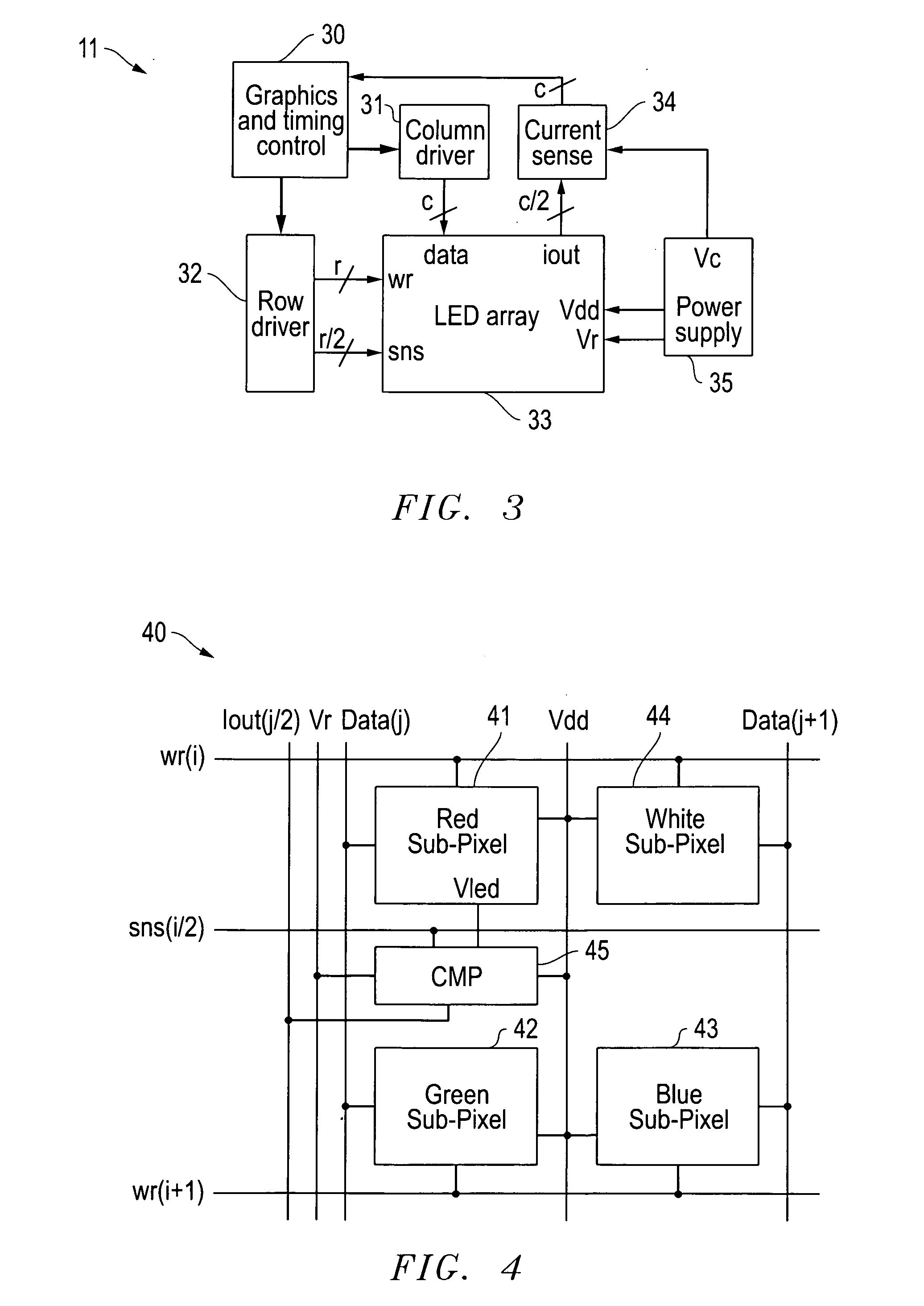
[0198]Display calibration systems and related methods are also disclosed that use the photo-sensitivity of LEDs to correct for variations between LEDs during initial production and over lifetime for display systems. Various embodiments are described with respect to the drawings below. Other features and variations can also be implemented, if desired, and related systems and methods can be utilized, as well.
[0199]In part, the disclosed embodiments relate to displays including arrays of LEDs that use the photo-sensitivity of the LEDs to correct for variations between LEDs during initial production and over lifetime of such a display. Such LED arrays can produce images directly as in LED billboards and sports arena scoreboards, and smaller Organic LED (OLED) displays, or can produce the backlight for LCD screens for instance. Variations in LED brightness and color can be compensated for in order for such a display to have uniform color and brightness. Such compensation, which is typically done in prior systems by measuring the optical output power of each individual LED or purchasing specially tested LEDs, is performed in the embodiments described below by simply measuring the signal induced on each LED by uniform incident light.
[0200]In one improved embodiment, the system infers the optical output power and optionally also the peak wavelength produced by each LED in an LED array for LED billboards and stadium displays for instance, or LCD backlighting, by measuring the photo-sensitivity of each such LED, comparing such sensitivity to the photo-sensitivity of the other LEDs in such array, and adjusting such LED drive current correction factors accordingly. Such correction factors can be initially generated during production of such LED array by measuring each such LED optical output power and peak wavelength directly, for instance, or by inferring each such LED optical output power and peak wavelength from photo-sensitivity and other measurements.
[0201]LEDs not only produce light with a specific peak wavelength when forward biased, but also forward bias when illuminated with light at or above such peak wavelength. The electrical power produced by a fixed incident optical power decreases with decreasing incident wavelength with the maximum power produced by incident light with a wavelength near such peak emission wavelength. Incident wavelengths above such peak emission wavelength produce roughly no electrical power in such LED. At a specific temperature, the relationship between voltage and current induced across a properly illuminated LED depends on the amount of illumination, the bandgap voltage of the semiconductor, and the resistive load placed across the LED. As the bandgap voltage of the semiconductor increases, the open circuit voltage (Voc) increases and the short circuit current (Isc) decreases. Since peak emission wavelength decreases with increasing bandgap voltage, the ratio of Voc to Isc can be measured to get an indication of wavelength variations between LEDs in an LED array.
[0202]The amount of light produced by different LEDs within a manufacturing lot or between lots when driven with a fixed current varies primarily due to differences in the optical path, such as transparency or alignment, and differences in the extent of imperfections in the structure of the light emitting region of the LED. Likewise, such differences similarly affect the photo-sensitivity of such LED when properly illuminated. Consequently, photo-sensitivity parameters, such as Voc and Isc, can be monitored to infer the amount of light that such LED will produce when driven with current.
[0203]Wavelength and output power from individual LEDs in an LED array can be compensated by correction coefficients to produce uniform intensity and color across such an array. Such correction coefficients determined during manufacturing of such an LED array by the methods described above, by directly measuring the intensity and wavelength of the light produced by each LED, or any other method, can be stored in memory in such a display. Likewise, photo-sensitivity parameters, such as Voc and Isc, produced in response to a light source with fixed parameters, can also be stored in such memory. Periodically, during the life of such a display, the LED array can be illuminated with a light source with the same or different parameters as the initial light source, the photo-sensitivity parameters can be measured, and differences between the initial and new photo-sensitivity parameter values can be used to modify the correction coefficients to correct for any additional shift in illumination from LEDs in such an LED array.
[0204]The light source used to calibrate an LED array during initial production can be direct or diffuse sunlight, a lamp that mimics the spectrum of sunlight, or any light source with a spectrum sufficient to generate reliably measurable photo-sensitivity parameters from LEDs of each color. To re-calibrate a large LED billboard or stadium display, for instance, the same light source with the same intensity can be used to measure the photo-sensitivity parameters under the exact same condition as when such a display was manufactured. Any shift in any photo-sensitivity parameter can be used directly to update corresponding correction coefficients. If precisely controlling the light source intensity is not possible, then comparing changes in one LED relative to the others enables uniform display intensity and color to be recreated. The user could simply manually adjust overall brightness.
[0205]For consumer devices such as an LCD television, calibration with a precise light source may not be possible. A close approximation could be diffuse sunlight, but the spectrum of sunlight varies with time day and year, and location. Additionally, such a device could be in an enclosed room with artificial lighting. In such a case, uniformity across LEDs of each color component can be produced, but the relative intensity between color components may not. The user in this case could manually adjust both overall brightness and hue to the desired levels.
[0206]The improved display calibration systems and related methods described herein address calibration issues for displays using arrays of LEDs directly or as backlights for illumination. And the calibration systems and related methods described herein greatly reduce or eliminate the need for teams of specially trained and equipped people to keep LED billboards and stadium displays calibrated during operation over time.
[0207]As stated above, this second embodiment can also be used with the techniques, methods and structures described with respect to the other embodiments described herein. For example, the calibration and detection systems and methods described with respect to this embodiment can be used within the other described embodiments, as desired. Further, the various illumination devices, light sources, light detectors, displays, and applications and related systems and methods described herein can be used with respect to calibration and detection systems and methods described in this second embodiment, as desired. Further, as stated above, the structures, techniques, systems and methods described with respect to this second embodiment can be used in the other embodiments described herein, and can be used in any desired lighting related application, including liquid crystal displays (LCDs), LCD backlights, digital billboards, organic LED displays, AMOLED (Active Matrix OLED) displays, LED lamps, lighting systems, lights within conventional socket connections, projection systems, portable projectors and/or other display, light or lighting related applications.
[0208]Turning now to the drawings, FIG. 14 is one example of display calibration system 1410 that comprises the display 1411 and light source 1414. Display 1411 comprises an array of light emitting diodes (LEDs) arranged as pixels 1412 for image illumination either directly in the case of OLED or conventional LED displays, or backlighting in the case of Liquid Crystal Displays (LCDs). Pixel 1412 preferentially comprises different color sub-pixels 1413, for instance red, green, and blue, to produce the wide gamut of colors typically necessary for accurate representation of images either directly in the case of OLED or LED displays, or modulated as in an LCD. Sub-pixel 1413 comprises an LED.
[0209]Light source 1414 can be direct or diffuse sunlight, or artificial light from a lamp with a precise emitted light spectrum. During the manufacturing of display 1411, light source 1414 illuminates display 1411 uniformly to calibrate the intensity and wavelength of light emitted from each pixel 1412 and to measure and store photo-sensitivity parameters such as Voc and Isc, or to simply measure and store photo-sensitivity parameters in which case the intensity and wavelength of all pixels 1412 are calibrated by some other means such as measuring the light produced by each such pixel and adjusting some compensation coefficients accordingly. After some period of use, preferentially the same light source 1414 again illuminates display 1411 and the photo-sensitivity parameters of the LED comprising each sub-pixel 1413, such as Voc and Isc, are again measured and preferentially compared to those stored during the manufacturing of such display 1411. Any shift in such photo-sensitivity parameters or preferentially any difference in shift of such parameters in one pixel 1412 relative to preferentially the average shift in all pixels 1412 causes such compensation coefficients to be adjusted inversely proportional in such one pixel 1412.
[0210]If the Isc of the LED comprising a red sub-pixel 1413 for instance, decreases by more than the average decrease of all red sub-pixels 1413, such red sub-pixel compensation coefficients are increased to produce more current to such red sub-pixel 1413 by an amount preferentially inversely proportional to the percentage difference in the Isc change between such red sub-pixel 1413 and the average Isc change from all red sub-pixels 1413 in display 1411. Since the intensity of illumination on display 1411 from light source 1414 is relatively difficult to control from manufacturing time to such re-calibration time, any change in compensation coefficients for red sub-pixels 1413 for instance, is preferentially normalized to the average Isc from all red sub-pixels 1413.
[0211]FIG. 14 is one example of many possible display calibration systems 1410. For example, pixel 1412 could comprise more or less sub-pixels 1413 and such sub-pixels 1413 could comprise more or less different colored LEDs including just one color. Display 1411 could be an LCD, an OLED display, or a conventional LED display or just portions of such displays. Light source 1414 could be a single light source or many light sources with the same or different spectrums.
[0212]FIG. 15 is an example block diagram of OLED display 1411 comprising LED array 1523 with R rows and C columns of sub-pixels 1413 typically arranged in pixels 1412 of one red, one green, one blue, and one white sub-pixel LED. LED array 1523 comprises R/2 rows and C/2 columns of such sub-pixels 1413. Each sub-pixel 1413 is configured to produce a certain amount of light by a combination of voltages on a particular WR (write) signal produced by row driver 1522 and DATA signal produced by column driver 1521. When a WR signal is high, the analog voltage on each DATA signal is programmed into the row of sub-pixels 1413 activated by the particular WR signal.
[0213]Power supply 1525 produces the main power Vdd and the ground Vg for LED array 1523. The voltage on such Vg signal is equal to zero volts during normal operation and during the Voc measurement of each sub-pixel 1413, and is elevated slightly above display 1411 ground during Isc measurements.
[0214]During calibration, graphics and timing control circuitry 1520 sequences row driver 1522 through rows of LED array 1523 by pulsing each SNS (sense) signal high. When one of the SNS signals from row driver 1522 goes high, the IVOUT signals from the LED array 1523 source current or voltage into IV sense 1524 for sub-pixels 1413 in the row activated by a particular SNS signal. Depending on the state of the voltage mode enable signal Ven, IV sense 1524 either will pass the voltages on the IVOUT signals to ADC 1526 or will short the IVOUT signals to Vg, convert the resulting currents to voltages, and forward the resulting voltages to ADC 1526. ADC 1526 together with timing information from graphics and timing control circuitry 1520 sequentially converts the voltages forwarded by IV sense 1524 to digital values, which are forwarded to graphics and timing control circuitry. 1520 for processing.
[0215]Graphics and timing control circuitry 1520 can receive Voc and Isc, and other calibration information from sub-pixels 1413, and can compare such information with previously stored such values to determine any changes necessary to correction coefficients. Graphics and timing control circuitry 1520 can use such correction coefficients to adjust the voltages programmed into sub-pixels 1413 to compensate for variations in light output from each sub-pixel 1413 relative to other sub-pixels 1413.
[0216]FIG. 15 is just one of many possible block diagrams for display 1411, which could be built using any one of a wide range of technologies including but not limited to discreet inorganic LED arrays or liquid crystals. Likewise, the block diagram for display 1411 built with OLEDs could be substantially different. For instance, with additionally circuitry in sub-pixels 1413, the SNS signals or the IVOUT signals could be eliminated, by using the WR and DATA signals during calibration. Additionally, the Vg could simply be system ground provided N sense 1524 circuitry was different.
[0217]FIG. 16 is an example block diagram of OLED pixel 1412 in LED array 1523 referenced by row coordinates I and I+1, and column coordinates J and J+1, and comprising red, green, blue, and white sub-pixels 1413. The circuitry in all sub-pixels is the same except the color of the included LED.
[0218]Signals WR(i) and DATA(j) program the light produced by red sub-pixel 1413, signals WR(i) and DATA(j+1) program the light produced by white sub-pixel 1413, signals WR(i+1) and DATA(j) program the light produced by green sub-pixel 1413, and signals WR(i+1) and DATA(j+1) program the light produced by blue sub-pixel 1413. All sub-pixels are powered by the voltage difference between Vdd and Vg.
[0219]FIG. 16 is just one of many possible pixel 1412 block diagrams. For instance, any combinations of colors or just one color could be used. Additionally, all sub-pixels could be accessed by one WR signal and one DATA signal if two enable signals select between the sub-pixels.
[0220]FIG. 17 is an example circuit diagram for sub-pixel 1413 and an individual current and voltage sense element in IV sense 1524 referenced by coordinate J. When producing light, LED 1744 is driven by the current through transistor 1740, which is set by the voltage stored on capacitor 1743 and the gate of transistor 1740. The voltage on capacitor 1743 is set to the voltage on DATA(j) signal when WR(i) signal is low. When WR(i) goes high, capacitor 1743 holds the voltage so that DATA(j) can be used to program the current in other rows of sub-pixels 1413 when other WR signals go low. All the sub-pixels 1413 connected to WR(i) are programmed simultaneously by all the DATA signals when WR(i) is low.
[0221]When SNS(i) goes high, the Voc and Isc induced across LED 1744 by incident light can be measured by IV sense 1524, after capacitor 1743 is discharged by setting WR(i) low and DATA(j) high. Voc is measured when graphics and timing control circuitry 1520 sets the Ven signal high, which tri-states the output of amplifier 1746 and causes power supply 1525 to hold Vg at zero volts. The voltage on IVOUT(j) passes through resistor 1745 and to the high impedance input of ADC 1526, which converts such voltage to a digital value and forwards such value to graphics and timing control circuitry 1520.
[0222]Isc is measured when graphics and timing control circuitry 1520 sets the Ven signal low, which enables amplifier 1746 and forces the voltage on IVOUT(j) to the voltage on Vg. The resulting current flows through resistor 1745 producing a voltage on Sout(j) proportional to the Isc induced on LED 1744 by incident light. Since the voltage on Sout(j) is lower than that on Vg and IVOUT(j), the negative supply for IV sense 1524 and ADC 1526 is set to be lower than Vg. Power supply 1525 can raise the voltage on Vg to some small voltage, such as one volt above the negative supply, for instance ground, for display 1411.
[0223]Although not associated with photo-sensitivity of LED 1744, characteristics of transistor 1740 can be measured by such sub-pixel 1413, IV sense 1524, and ADC 1526 circuitry, and compensated by graphics and timing control circuitry 1520. After a voltage is programmed across capacitor 1743, the corresponding current produced by transistor 1740 can be measured when SNS(i) high and Ven is low. The voltage on IVOUT(j) is forced to the voltage on Vg by amplifier 1746 and resistor 1745 with the resulting current flowing through resistor 1745, which produces a voltage on SOUT(j) proportional to transistor 1740 current. Such voltage can be digitized by ADC 1526 and processed by graphics and timing control circuitry 1520, which can compensate for variations between transistors 1740 in all sub-pixels 1413.
[0224]FIG. 17 is one of many possible circuit diagrams for sub-pixels 1413 and IV sense 1524. For instance, sub-pixel 1413 could include additional circuitry to compensate for transistor 1740 variations without involving graphics and timing control circuitry 1520. Additionally, to detect LED 1744 Voc and Isc in response to incident light, sub-pixel 1413 could include more complex circuitry to buffer such signals prior to leaving such sub-pixel 1413.
[0225]FIG. 18 is an example architectural diagram for display 1411 that uses conventional discreet semiconductor LEDs, which comprises an array of LED driver ICs 1850 with associated LEDs 1851 connected serially to each other and to a network interface (I/F) IC 1852. Network interface IC 1852 connects to graphics controller 1853 through control and data busses. The array in this example has N columns and M rows of driver ICs 1850 each connected to P LEDs 1851. With P equal to 16 and three LEDs per pixel, N and M would equal 120 and 3240 respectively for an HD display with 1920×1080 resolution. For a standard 48 foot by 14 foot bill board with 3 LEDs per pixel, and P equal to 16, N would equal 48 and M would equal 672.
[0226]LED's 1851 could all be the same color or could be divided between red, green, and blue for instance. For an RGB display, the different colors could be arranged in different ways. One example is to organize the display in groups of 3 rows with each row in each group being a different color.
[0227]Graphics controller 1853 produces the data to be displayed digitally, which is forwarded to network interface IC 1852. Network interface IC 1852 serializes the data, which is sent through the chain of driver ICs 1850 in a time division multiplexed data frame. Each driver IC 1850 is assigned specific time slots from which image data is received and calibration information can be sent. The data frame repeats at the video frame rate, which enables each driver IC 1850 to update the drive current to each LED 1851.
[0228]Driver IC 1850 can further process the data to be displayed with correction coefficients that adjust the drive current to each LED 1851 such that brightness and color are uniform across display 1411. Such correction coefficients can be stored in graphics controller 1853, downloaded through network interface IC 1852 to driver ICs 1850 each time display 1411 is turned on, and updated periodically by graphics controller 1853. Such correction coefficients can be created and updated periodically over the life of display 1411 by graphics controller 1853 using individual LED photo-sensitivity parameters such Voc and Isc measured by driver ICs 1850 on commands from graphics controller 1853, for instance.
[0229]FIG. 18 is one of many possible architectural diagrams. For instance, each driver IC 1850 could be connected directly to graphics controller 1853 through a multiplexer either serially or in parallel. The LED drivers could be made from discreet components instead of driver IC 1850. The data for the LED drivers could even be communicated with analog voltages instead of digital values. Additionally, the creation and updating of correction coefficients could be performed by driver IC 1850, or processing of the data to be displayed with correction coefficients could be performed by graphics controller 1853 for instance.
[0230]FIG. 19 is an example block diagram for driver IC 1850, which in this example drives sixteen LEDs 1851 and comprises network interface 1960, timing and control circuitry 1961, and sixteen output drivers 1964. Timing and control circuitry 1961 further comprises IV sense block 1962 and correction matrix 1963. Output driver 1964 further comprises pulse width modulator 1965, and current source 1966.
[0231]Network interface 1960 accepts serial input data from upstream and produces serial data for downstream driver ICs 1850 as shown in FIG. 18. Network interface 1960 further recovers the clock (CK) from the data, and detects and synchronizes to the input data frame timing. Most received serial data is retransmitted, however, data in the assigned timeslots are forwarded to timing and control circuitry 1961. Calibration information, such Voc and Isc, among other things is produced by timing and control circuitry 1961 and forwarded to network interface 1960 for transmission in the assigned timeslots from which LED 1851 illumination data was removed.
[0232]Timing and control circuitry 1961 manages the functionality of driver IC 1850. Illumination data for. LEDs 1851 is buffered, processed, delayed, and forwarded at the appropriate time to the sixteen output drivers 1964. Such processing can include among other things adjustment of the illumination data to compensate for variations between LEDs to produce uniform brightness and color across display 1411. Matrix 1963 can comprise correction coefficients that when combined with the illumination data produce the data forwarded to output drivers 1964, which have pulse width modulators 1965 that produce logic level signals that turn current sources 1966 on and off to LEDs 1851. The frequency of such PWM signals is typically equal to the serial data frame rate and the video frame rate with the duty cycle related to the digital value from matrix 1963.
[0233]Timing and control circuitry 1961 has access to both terminals of all 16, in this example, LEDs connected to driver IC 1850 through IV sense block 1962, which among other things can measure Voc and Isc produced across LEDs 1851 in response to incident light. The anodes of all sixteen LEDs in this example can be tied together to a single supply voltage Vd, or can be connected to different supply voltages. In the case all sixteen LEDs 1851 are of one color, all anodes preferentially would be connected together. In the case such sixteen LEDs 1851 are of different colors, each such different color LED 1851 would preferentially be connected to each such different supply voltage.
[0234]FIG. 19 is just one example of many possible driver IC 1850 block diagrams. For instance, network interface 1960 would not be needed if each driver IC 1850 in FIG. 18 were directly connected to graphics controller 1853. With the serial configuration shown in FIG. 18, network interface 1960 would not need to recover a clock from data if another input was used to accept a clock input. Likewise, if a frame clock input was provided, network interface 1960 would not need to synchronize to the serial input frame timing. Additionally, the function of matrix 1963 could be performed by graphics controller 53, which would eliminate the need for such matrix 1963 in driver IC 1850. Modulator 1965 would not be needed if LEDs 1851 were driven with variable current for fixed amount of times, for instance.
[0235]FIG. 20 is an example block diagram of correction matrix 1963 that can correct for variations in light intensity produced by a pixel 1412 comprising red, green, and blue LEDs 1851 to produce relatively uniform brightness and color across a display 1411. Matrix 1963 comprises memory 2070 that can store correction coefficients Cr, Cg, and Cb, which are combined by multipliers 2071 with the red, green, and blue illumination data respectively from graphics controller 1853 to produce the illumination data forwarded to modulators 1965 controlling red, green, and blue LEDs 1851 respectively. Such correction coefficients are typically relatively large, which produce adjustments in the illumination data to compensate for variations between LEDs 1851.
[0236]Memory 2070 can be made from SRAM, DRAM, FLASH, registers, or any other form of read-writable semiconductor memory. Such correction coefficients periodically can be modified by graphics controller 1853, driver IC 1850, or any other processing element in display 1411 to adjust for changes in LED 1851 characteristics for instance over temperature or lifetime. Typically, such correction coefficients are downloaded into memory 2070 from graphics processor 1853 every time display 1411 is turned on. Such correction coefficients are typically modified to compensate for LED 1851 aging effects by graphics controller 1853 or driver IC 1850 after some fixed number of hours of use, after every use, or on demand.
[0237]Multipliers 2071 scale the illumination data from graphics controller 1853 by multiplying each color component by the corresponding correction coefficient. Such multiplication can be performed by discreet hardware in bit parallel or bit serial form, in an embedded microcontroller, or by any other means. Preferentially, one hardware multiplier comprising a shifter and an adder performs all three multiplications each video frame. As such, FIG. 20 is just one of many possible block diagrams for correction matrix 1963.
[0238]FIG. 21 is an example block diagram for correction matrix 1963 that can correct for variations in both light intensity and wavelength produced by a pixel 1412 comprising red, green, and blue LEDs 1851 to produce uniform brightness and color across a display 1411. Matrix 1963 comprises memory 2070 that can store nine correction coefficients with three such coefficients for each color component produced. Coefficients Crr, Cgg, and Cbb would typically be effectively the same as Cr, Cg, and Cb from FIG. 20 to adjust for intensity variations in LEDs 1851, while the remaining coefficients (Crg, Crb, Cgr, Cgb, Cbr, Cbg) compensate for wavelength variations.
[0239]For instance, if the red illumination data from graphics controller 1853 was intended for an LED 1851 with a wavelength of 650 nm and the connected LED 1851 wavelength was exactly 650 nm, coefficients Cgr and Cbr would be zero and Crr would be close to one. If such connected LED 1851 wavelength was 640 nm and had the same intensity as the just previous example, Crr would be slightly smaller than in the just previous example and Cgr and Cbr would be non-zero, which would produce some light from such green and blue LEDs 1851. The wavelength of the combination of light from such red, green, and blue LEDs 1851 would be perceived the same as mono-chromatic light from a single red LED 1851 emitting at precisely 650 nm.
[0240]Memory 2070 and multipliers 2071 can operate and be implemented as described for FIG. 20. Adder 2180 sums the multiplication results from the three connected multipliers 2071 to produce the illumination data forwarded to modulators 1965. Such adders 2080 can be implemented in hardware or software, or be performed bit parallel or bit serial. Preferentially, such three adders 2080 are implemented with common bit serial hardware that performs such three additions sequentially each video frame. As such FIG. 21 is just one of many possible intensity and wavelength correction matrix 1963 block diagrams.
[0241]FIG. 22 is an example block diagram of IV sense block 1962 in timing and control block 1961 of driver IC 1850, which can measure LED 1851 photo-sensitivity parameters, such as Voc and Isc, when current source 1966 is off. Following the example in FIG. 18, the anodes of sixteen LEDs 4851 represented by the signals Vled(1:16) are connected to multiplexer 2294 with one such Vied signal selected to pass through. Such output of multiplexer 2294 is connected to an input of multiplexer 2291 and to the negative terminal of amplifier 2292 and resistor 2293. Such multiplexers 2291 and 2294 comprise switches that connect input to output and allow current to flow in both directions for the selected input. The output of amplifier 2292 is also connected to multiplexer 2291 the output of which is connected to analog to digital converter (ADC) 2290.
[0242]Amplifier 2292 and resistor 2293 form a trans-impedance amplifier which forces the anode of the LED 1851 selected by multiplexer 2294 to the same voltage as signal Vd, which is connected to the positive terminal of amplifier 2292. The resulting current flows through resistor 2293 producing a voltage proportional to the selected LED 1851 short circuit current Isc, which can be digitized by ADC 2290 if selected by multiplexer 2291. Alternatively, the open circuit voltage Voc of the LED 1851 selected by multiplexer 2294 can be digitized by ADC 2290 if multiplexer 2291 selects such signal. The power supply for IV sense block 1962 is made to be higher than Vd since the output of amplifier 2292 may go higher than Vd.
[0243]FIG. 22 is just one of many possible block diagrams for circuitry to measure photo-sensitivity parameters of LEDs 1851. For instance, a range of LED 1851 current and voltage characteristic could be measured by controlling the positive input to amplifier 2292 with a digital to analog converter (DAC). If each LED 1851 had a dedicated IV sense block 1962, no multiplexer 2294 would be needed. Additionally, Voc could be measured by adjusting the voltage on the positive terminal of amplifier 2292 until no current flows through resistor 2293. Further, switched capacitor and sample and hold techniques could be implemented which would have a completely different architecture.
[0244]FIG. 23 is an example block diagram of display 1411 implemented with a liquid crystal display (LCD) and an LED backlight, which comprises LCD array 2300, LED array 2301, graphics and timing control circuitry 2302, row driver 2303, column driver 2304, and backlight driver network 2305.
[0245]In this example, LCD array 2300 has R rows and C columns of elements with row driver 2303 producing R number of WR signals and column driver 2304 producing C number of DATA signals. Graphics and timing control circuitry 2302 provide data and timing to both row driver 2303 and column driver 2304 in a similar manner to an OLED display as described in FIG. 15.
[0246]In this example, LED array 2301 comprises M rows and N columns of LEDs driven by backlight driver network 2305, which comprises a number of LED driver ICs connected together as in the LED display illustrated in FIG. 18. LCD array 2300 comprises pixel elements that control the amount of light that can pass through. LED array 2301 produces the light that is selectively passed through LCD array 2300. When photo-sensitivity parameters, such as Voc and Isc of LEDs 1851 in LED array 2301 are measured, row driver 2303 and column driver 2304 configure LCD array 2300 to be transparent.
[0247]FIG. 23 is just one of many possible block diagrams for display 1411 based on LCD and LED backlighting technology. For instance, all LED elements in LED array 2301 could be directly connected to graphics and timing control circuitry 2302 through a multiplexer instead of backlight driver network 2305.
[0248]FIG. 24 is an example circuit diagram for the LCD pixel element in LCD array 2300 and the associated row driver 2303 and column driver 2304, which comprises transistor 2410, capacitor 2411, liquid crystal 2412, buffer amplifier 2413, and inverter 2414. Such pixel element is repeated horizontally C times and vertically R times to produce LCD array 2300, with each row of pixel elements controlled by a WR signal from an inverter 2414 in row driver 2303 and each column of pixel elements connected to a single DATA signal from buffer amplifier 2413 in column driver 2304.
[0249]The transparency of liquid crystal 2412 is controlled by the voltage across capacitor 2411, which is set by driving DATA(j) with the desired voltage and then pulsing WR(i) high to make transistor 2410 conductive. When WR(i) is high, capacitor 2411 is charged to the voltage on DATA(J), which is driven by buffer amplifier 2413. When photo-sensitivity parameters, such as Voc and Isc of LEDs 1851 in LED array 2301 are measured, liquid crystal 2412 for every pixel element in LCD array 2300 is made transparent by preferentially setting all WR signals high simultaneously and setting the voltage on all DATA signals to the value that makes liquid crystal 2412 transparent.
[0250]FIG. 24 is just one of many possible LCD array 2300, row driver 2303, and column driver 2304 circuit diagrams. For instance, some pixel elements contain multiple transistors to compensate for transistor 2410 variations and speed up the write process.
[0251]Numerous variations and modifications will become apparent to those skilled in the art once the above disclosure is fully appreciated.
Example
Third Embodiment
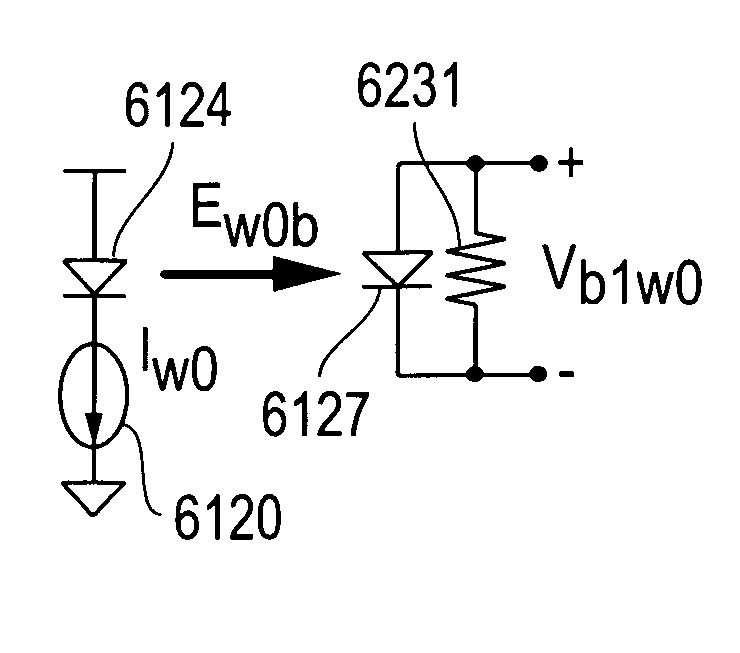
[0252]LED calibration systems and related methods are also disclosed that use the photo-sensitivity of LEDs to correct for variations between LEDs during initial production and over the lifetime of systems using LEDs. Various embodiments are described with respect to the drawings below. Other features and variations can also be implemented, if desired, and related systems and methods can be utilized, as well.
[0253]In part, the disclosed embodiments relate to using the photo-sensitivity of an LED to determine emission parameters such as intensity and wavelength. Applications for the disclosed embodiments include solid state lamps, LCD backlights, and LED displays for instance. Variations in LED brightness and wavelength should be compensated for in order for such devices to have uniform color and brightness. Such compensation, which is typically done by measuring the optical output of each individual LED with a camera or purchasing specially tested LEDs, is performed by simply measuring the signal induced on each LED by light from other LEDs in the device or from an additional light source.
[0254]The disclosed embodiments include methods to set the color or color temperature produced by a group of LEDs during the manufacturing of a device such as a lamp, an LED display, or an LCD backlight, and maintaining such color or color temperature over the operating life of such a device. The methods involve measuring the intensity and wavelength of light produced by each LED within a group of LEDs and adjusting the amount of light generated by each LED to produce precise color and intensity from the group of LEDs.
[0255]Two methods that operate some of the LEDs in photovoltaic or photoconductive mode to measure the light intensity produced by other LEDs in the group are presented. The first method that uses an additional light source as a reference determines the light intensity emitted from each LED relative to such reference, while the second method determines the light intensity emitted from each LED relative to each other. As such, the first method can produce a precise color and intensity from each group of LEDs, while the second method can only produce a precise color.
[0256]Both intensity measurement methods typically comprise two steps and can be used to calibrate devices during both manufacturing and over lifetime. The first step of the first method illustrated in FIGS. 25A-D and the first step of the second method illustrated in FIG. 27A-D can be performed in a manufacturing environment on a special control device that has all LEDs manually adjusted to produce the desired light intensities. The results of the first step on such control device are then used in the second step of the first method illustrated in FIGS. 26A-D and the second step of the second method illustrated in FIGS. 28A-D on production devices to determine the actual emitted light intensities.
[0257]Both intensity measurement methods can also be used to maintain a precise color produced by a group of LEDs and uniform intensity from an array of groups of LEDs, for instance pixels in an LED display, LCD backlight, or LED lamp, over time. The first step of both methods is typically performed on a device after such device has been calibrated during manufacturing and the second step is performed in the field at periodic intervals. The reference light source for the first intensity measurement method can be ambient light.
[0258]Emission intensity is measured in all cases by measuring the photocurrent produced in the longest wavelength LED within the group of LEDs by light from the other LEDs and in the first method from an additional reference light source. For instance, in an LED array for an LED display or backlight, according to the example shown for the first method, the red LED in a pixel measures the light from the blue and green LEDs in the same pixel, and from the reference light source. Next, the red LED in an adjacent pixel measures the light from the first red LED and the reference light source. Such measured light can be reflected off a mirror for an LED display during manufacturing or off the waveguide or diffuser in an LED backlight for instance. In the field, such light can be scattered by the LED packages or enclosures or by any other means.
[0259]In the example shown for the second method, which includes two red LEDs and one white LED in an LED lamp for instance, a first red LED measures the light from a second red LED and from the white LED. Next, light from the second LED measures the light from the first LED and from the white LED. Both the first and second intensity measurement methods can be used for any groups of LEDs in any types of products with the difference between the methods being the presence or absence of a reference light source. The second method could be used in an LED display or backlight to produce precise color and uniform intensity from all pixels by daisy chaining the measurements sequentially across such LED array.
[0260]The example intensity measurement methods are divided into two steps which measure the differences in relative intensity between a known good measurement and the unknown measurement. For instance, during manufacturing, a control device with the desired output intensities is measured to determine what the relative photocurrents should be. Using the first method, the ratios of the photocurrent in a first LED produced by the light from the other LEDs over the photocurrent produced by the reference light source generate coefficients used for the second step. Provided the ratio of intensities from the reference light source in the first and second steps is known, the unknown LED intensities in the second step can be determined. Likewise, using the second method, the ratios of photocurrents induced on one LED by the two other LEDs in a calibrated control device generate coefficients used in the second step. In the second step, the difference in the ratios from the first step determines the difference in relative unknown intensities between the two LEDs.
[0261]When the first or second method is used to calibrate a device over time, the first step determines what ratios of photocurrents should be and over time the second step determines what they are. The change in such ratios determines the change in actual emission intensity. Since only ratios currents measured at one time are compared to ratios of currents at another time, any changes in operating conditions cancel out. For instance, such measurements are independent of temperature differences.
[0262]The method presented to measure emission wavelength illuminates each LED with two different wavelengths of lights, such as a light wavelength slightly above and below the anticipated peak emission wavelength range, and measures the resulting photocurrent. Since the responsivity of an LED drops off dramatically for incident wavelengths longer than the peak emission wavelength, the difference in induced photocurrents is directly related to the peak emission wavelength. FIGS. 31A-C provide a graphical illustration of LED responsivity as a function of incident wavelength and the resulting photocurrent differences.
[0263]Since LED emission wavelength does not vary significantly over time, such wavelength measurements can just be performed on a production line. As in the two emission intensity methods, such wavelength measurement should first be done on a control device with known emission intensity to calibrate the production test setup. Subsequent measurements of devices with unknown emission wavelengths, will be relative to the control device results.
[0264]Once the emission wavelengths and the emission intensity or relative emission intensity between a group of LEDs is known, color correction coefficients can be determined that adjust the emission intensity of light from each LED within a group of LEDs to produce a precise color and optionally a precise intensity from such group of LEDs. FIG. 29 illustrates hardware to implement the calibration methods. FIG. 30 illustrates color correction coefficients and hardware to correct for emission intensity variations, while FIG. 32 illustrates such coefficients and hardware to correct for both emission intensity and wavelength variations between the red, green, and blue LEDs associated with a pixel in an LED display or a triplet in an LCD backlight.
[0265]Although such calibration methods are appropriate for any devices that contain groups of LEDs, of particular interest are LCDs that use Field Sequential Color (FSC). FIG. 33 illustrates a simplified block diagram of a conventional LCD, while FIG. 34 illustrates such a diagram for a FSC LCD. While a conventional LCD has white backlight that is filtered into red, green, and blue components by special color filters, a FSC LCD eliminates the costly color filters and sequences each color component at three times the conventional frame rate or more. Such FSC LCDs require red, green, and blue backlights and as such are a primary application for the color calibration methods described herein.
[0266]The improved methods herein address problems associated with devices using groups of different colored LEDs directly or as backlights for illumination. Such calibration methods reduce the need for specially binned LEDs for the production of lamps, displays, or backlights, and maintain the color or color temperature of the light produced over the operating life of the device.
[0267]As stated above, this third embodiment can also be used with the techniques, methods and structures described with respect to the other embodiments described herein. For example, the calibration and detection systems and methods described with respect to this embodiment can be used within the other described embodiments, as desired. Further, the various illumination devices, light sources, light detectors, displays, and applications and related systems and methods described herein can be used with respect to calibration and detection systems and methods described in this third embodiment, as desired. Further, as stated above, the structures, techniques, systems and methods described with respect to this third embodiment can be used in the other embodiments described herein, and can be used in any desired lighting related application, including liquid crystal displays (LCDs), LCD backlights, digital billboards, organic LED displays, AMOLED (Active Matrix OLED) displays, LED lamps, lighting systems, lights within conventional socket connections, projection systems, portable projectors and/or other display, light or lighting related applications.
[0268]Turning now to the drawings, FIGS. 25A-D in association with FIGS. 26A-D illustrate one possible method for calibrating the intensity of light produced by each LED within a group of LEDs to produce a specific blended color. Such group of LEDs could be any combination of colors, but as an example comprise red, green, and blue LEDs. Specifically, in such example, LEDs 2510, 2520, and 2530 could comprise the red, green, and blue light sources respectively in an LED display pixel or LCD backlight triplet. LED 2540 comprises the red light source in an adjacent LED display pixel or backlight triplet.
[0269]FIGS. 25A-D illustrate the first step in such calibration method, which can be performed on one special device comprising such group of LEDs that is representative of many such devices produced on a manufacturing line for instance. Alternatively, such first step could be performed on a device that is to be re-calibrated some time later using the second step in such calibration method illustrated in FIGS. 26A-D.
[0270]The following equations are associated with FIGS. 25A-D. In particular, equations 1 and 2 are associated with FIG. 25A. Equations 3A and 3B are associated with FIG. 25B. Equations 4A and 4B are associated with FIG. 25C. And equations 5A and 5B are associated with FIG. 25D.
Vr0n=E0Rr0 [EQ. 1]
Vr1n=E0Rr1 [EQ. 2]
Vr0gn=EgdRr0Cr0g=Egd(Vr0n/E0)Cr0g [EQ. 3A]
Cr0g=(Vr0gn/Vr0n)(E0/Egd) [EQ. 3B]
Vr0bn=EbdR0Cr0b=Ebd(Vr0n/E0)Cr0b [EQ. 4A]
Cr0b=(Vr0bn/Vr0n)(E0/Ebd) [EQ. 4B]
Vr1r0n=Er0dRr1Cr1r0=ErOd(Vr1n/E0)Cr1r0 [EQ. 5A]
Cr1r0=(Vr1r0n/Vr1n)(E0/ErOd) [EQ. 5B]
[0271]The light emitted from LEDs 2510 (red), 2520 (green), and 2530 (blue) is adjusted by varying current sources 2511, 2521, and 2531 to produce the desired light intensities Egd, Ebd, and Er0d from the green, blue, and red LEDs 2520, 2530, and 2510 respectively as shown in FIGS. 25B-D. Light source 2550 is adjusted to produce a fixed intensity E0, which illuminates LEDs 2510 and 2540, induces photo-currents proportional to incident light intensity, and produces the nominal voltages Vr0n and Vr1n across resistors 2512 and 2542 respectively as shown in FIG. 25A. Likewise, LEDs 2520 and 2530 illuminate LED 2510 as shown in FIGS. 25B-C and LED 2510 illuminates LED 2540 as shown in FIG. 25D to produce the nominal voltages Vr0gn, Vr0bn, and Vr1r0n respectively across resistors 2512 and 2542. Preferably, the resistance of resistors 2512 and 2542 should be small enough such that the induced voltages do not significantly forward bias LEDs 2510 and 2540.
[0272]The responsivities Rr0 and Rr1 of LEDs 2510 and 2540 to incident light from light source 2550 as shown in equations 1 and 2 respectively are equal to the ratios of the induced voltages Vr0n and Vr1n over the incident light intensity E0. As shown in equations 3A-B, the voltage Vr0gn induced across resistor 2512 by light from LED 2520 is equal to the light intensity Egd times such responsivity Rr0 times a correction coefficient Cr0g. Likewise, as shown in equations 4A-B, the voltage Vr0bn induced across resistor 2512 by light from LED 2530 is equal to the light intensity Ebd times such responsivity Rr0 times the correction factor Cr0b. Such correction factors Cr0g and Cr0b take into account differences in emitted light wavelength and optical attenuation between light from light source 2550, LED 2520, and LED 2530 and incident on LED 2510. For instance, light source 2550 could produce red light while LED 2520 and 2530 produce green and blue respectively. Additionally, light source 2550 could shine directly on LED 2510 while light from LEDs 2520 and 2530 could be indirect since such LEDs could be mounted adjacent to each other. Alternatively, light from LEDs 2510, 2520, and 2530 could be reflected by a mirror in the case of an LED display or by a light diffusion film in the case of an LCD backlight. As shown in equation 3B, when equation 3A is combined with equation 1, such correction coefficient Cr0g is equal to the ratio of the measured voltages Vr0gn over Vr0gn times the ratio of the known light intensities B0 over Egd. Likewise, when equation 1 is substituted into equation 4A, Cr0b is expressed as a function of measured voltages and known light intensities as shown in equation 4B.
[0273]As in equations 3A-B and 4A-B, equations 5A-B relate the nominal voltage Vr1r0n induced across resistor 2542 by light from LED 2510 with the desired intensity Er0d. Substituting equation 2 into equation 5A results in the correction factor Cr1r0 being expressed as a function of measured voltages and known light intensities as shown in equation 5B.
[0274]With known values for such correction coefficients from a device, such as an LED display or LCD backlight, with emitted intensities adjusted to the desired values, the color point of such devices can be adjusted to a fixed point on a manufacturing line and maintained in the field following the second step in the calibration process illustrated in FIGS. 26A-D. The procedure illustrated in FIGS. 26A-D is performed on a different device with LEDs 2510, 2520, and 2530 emitting unknown intensities Er0, Eg, and Eb respectively and light source 2550 emitting either the same or known intensity on a manufacturing line for instance or an unknown intensity in the field from ambient light for instance.
[0275]The following equations are associated with FIGS. 26A-D. In particular, equations 6 and 7 are associated with FIG. 26A. Equations 8A, 8B and 8C are associated with FIG. 26B. Equations 9A, 9B and 9C are associated with FIG. 26C. And equations 10A, 10B and 10C are associated with FIG. 26D.
Vr0=E1R0 [EQ. 6]
Vr1=E1Rr1 [EQ. 7]
Vr0g=EgRr0Cr0g=Eg(Vr0/E1)Cr0g [EQ. 8A]
Vr0g=Eg(Vr0/E1)(Vr0gn/Vr0n)(E0/Egd) [EQ. 8B]
Eg/Egd=(Vr0g/Vr0)(Vr0n/Vr0gn)(E1/E0) [EQ. 8C]
Vr0b=EbRr0Cr0b=Eb(Vr0/E1)Cr0b [EQ. 9A]
Vr0b=Eb(Vr0/E1)(Vr0gbn/Vr0n)(E0Ebd) [EQ. 9B]
Eb/Ebd=(Vr0b/Vr0)(Vr0nVr0bn)(E1/E0) [EQ. 9C]
Vr1r0=Er0Rr1Cr1r0=Er0(Vr1/E1)Cr1r0 [EQ. 10A]
Vr1r0=Er0(Vr1/E1)(Vr1r0/Vr1n)(E0/Er0d) [EQ. 10B]
Er0/Er0d=(Vr1r0/Vr1)(Vr1n/Vr1r0n)(E1/E0) [EQ. 10C]
[0276]Equations 6 and 7 relate the responsivities Rr0 and Rr1 of LEDs 2510 and 2540 respectively to the intensity E1 emitted by light source 2550. Equation 8A shows the voltage Vr0g induced across resistor 2512 by the unknown light intensity Eg from LED 2520 being equal to Eg times Rr0 times the correction coefficient Cr0g. Substituting equation 6 into equation 8A and replacing Cr0g with equation 3 results in the ratio of the actual emitted intensity Eg over the desired emitted intensity Egd equal to the ratio of the measured voltages Vr0g over Vr0 times the ratio of the nominal voltages Vr0n over Vr0gn measured as illustrated in FIGS. 25A-D times the ratio of intensities E1 over E0 emitted by light source 2550, as shown in equations 8B an 8C. Likewise, equations 9A-C and 10A-C express the ratios of the unknown intensities Eb and Er0 over the desired intensities Ebd and Er0d respectively as a function of measured voltages and known light intensities emitted from light source 2550.
[0277]Since the light intensity produced by an LED changes over time, a device such as an LED display or an LCD backlight with red, green, and blue LEDs, should be re-calibrated after some time to maintain the precise color calibrated during production of such device. In such a field re-calibration light source 2550 may be daylight or office ambient light of unknown intensity. In such cases, the ratio E1 over E0 is unknown but is the same for equations 8A-C, 9A-C, and 10A-C so the relative intensity of light produced by LEDs 2510, 2520, and 2530, and consequently the color can be maintained. Likewise, the intensity of light produced by all such pixels or backlight triplets can be kept uniform since the ratio of E1 over E0 should be the same for all such pixels or triplets.
[0278]FIGS. 27A-D in association with FIGS. 28A-D illustrate a method of calibrating the light produced by a group of LEDs 2510, 2520, and 2540 to produce a fixed color similar to such method illustrated in FIGS. 25A-D and 26A-D but without the reference light source 2550. In the method illustrated in FIGS. 27A-D and 28A-D the relative intensity of light produced by each LED can be controlled but not the absolute intensity of the group of LEDs 2510, 2520, and 2540. In this example, LEDs 2510 and 2540 are shown to be red, while LED 2520 is shown to be a white LED. An example application for such a group of LEDs is a lamp emitting white light with a low color temperature similar to that of an incandescent light bulb.
[0279]The following equations are associated with FIGS. 27A-D. In particular, equations 11, 12, 13A and 13B are associated with FIGS. 27A-B. And equations 14, 15, 16A and 16B are associated with FIGS. 27C-D.
Vr0wn=EwdRr0CrOw [EQ. 11]
Vr0r1n=Er1dRr0CrOr1 [EQ. 12]
Vr0wn/Vr0r1n=(Ewd/Er1d)(Cr0w/Cr0r1) [EQ. 13A]
Cr0w/Cr0r1=(Vr0wn/Vr0d1n)(Er1d/Ewd) [EQ. 13B]
Vr1wn=EwdRr1Cr1w [EQ. 14]
Vr1r0n=ErOdRr1Cr1r0 [EQ. 15]
Vr1wnVr1r0n=(Ewd/Er0d)(Cr1w/Cr1r0) [EQ. 16A]
Cr1w/Cr1r0=(Vr1wn/Vr1r0n)(Er0d/Ewd) [EQ. 16B]
[0280]The following equations are associated with FIGS. 28A-D. In particular, equations 17, 18, 19A and 19B are associated with FIGS. 28A-B. And equations 20, 21, 22A, 22B and 23 are associated with FIGS. 28C-D.
Vr0w=EwRr0Cr0w [EQ. 17]
Vr0r1=Er1Rr0Cr0r1 [EQ. 18]
Vr0r1Nr0w=(Er1/Ew)(Cr0r1/Cr0w) [EQ. 19A]
Er1Ew=(Vr0r1/Vr0w)(Cr0w/Cr0r1)=(Vr0r1Nr0w)(Vr0wnNr0r1n)(Er1dEwd) [EQ. 19B]
Vr1w=EwRr1Cr1w [EQ. 20]
Vr1r0=Er0Rr1Cr1r0 [EQ. 21]
Vr1r0/Vr1w=(Er0/Ew)(Cr1r0/Cr1w) [EQ. 22A]
Er0/Ew=(Vr1r0/Vr1w)(Cr1w/Cr1r0)=(Vr1r0/Vr1w)(Vr1wn/Vr1r0n)(Er0d/Ewd) [EQ. 22B]
Er0/Er1=(Er0/Ew)/(Er1/Ew)[EQ. 23]
[0281]The first step in such calibration method as shown in FIGS. 27A-D is to adjust current sources 2511, 2521, and 2541 to produce the desired light intensities Er0d, Ewd, and Er1d from LEDs 2510, 2520, and 2540 respectively as shown in FIGS. 27A-D. Then the light from LED 2520 and LED 2540 are measured by LED 2510, which produce the nominal voltages Vr0wn and Vr0r1n respectively across resistor 2512 as shown in FIGS. 27A and 27B. Equations 11 and 12 illustrate the relationship between such voltages, emitted powers, responsivity, and correction factors. Equations 13A-B take the ratio of equation 11 over 12 to produce the ratio of correction coefficients Cr0w over Cr0r1 expressed as a function of the ratio of nominal voltages Vr0wn over Vr0r1n times the ratio of desired emission intensities Er1d over Ewd.
[0282]Next the light from LEDs 2520 and 2510 are measured by LED 2540, which produce the nominal voltages Vr1wn and Vr1r0n respectively across resistor 2542 as shown in FIGS. 27C and 27D. Equations 14 and 15 relate such voltages to emitted powers, responsivity, and correction factors. Equations 16A-B take the ratio of equation 14 over 15 to produce the ratio of correction coefficients Cr1w over Cr1r0. Once such ratios of correction coefficients are known, the relative intensities of light produced by similar such devices on a manufacturing line can be determined and adjusted to produce a desired color. Likewise, such devices can be re-calibrated in the field after use to maintain the desired color.
[0283]FIGS. 28A-D illustrate the second step in the method to calibrate color without a reference light source. In such second step, LEDs 2520 and 2540 sequentially illuminate LED 2510 with unknown light intensities Ev, and Ed respectively, which produce voltages Vr0w, and Vr0r1 respectively across resistor 2512 as shown in FIGS. 28A and 28B. Equations 17 and 18 relate the induced voltages Vr0w and Vr0r1 to the emitted powers Ew and Er1, the responsivity Rr0, and the correction coefficients Cr0w and Cr0r1 respectively. Equations 19A-B take the ratio of equation 18 over 17 and substitutes equation 13B for the ratio of correction coefficients Cr0w over Cr0r1 to express the ratio of emitted intensities Er1 over Ew as a function of measured voltages and desired emitted intensities.
[0284]Next, LEDs 2520 and 2510 sequentially illuminate LED 2540 with unknown light intensities Ew and Er0 respectively, which produce voltages Vr1w and Vr1r0 respectively across resistor 2542 as shown in FIGS. 28A-D. Equations 20 and 21 relate the induced voltages Vr1w and Vr1r0 to the emitted powers Ew and Er0, the responsivity Rd, and the correction coefficients Cr1w and Cr1r0 respectively. Equations 22A-B take the ratio of equation 21 over 20 and substitutes equation 16B for the ratio of correction coefficients Cr1w over Cr1r0 to express the ratio of emitted intensities Er0 over Ew as a function of measured voltages and desired emitted intensities. Equation 23 expresses the ratio of Er0 over Er1 as the ratio of equation 22B over equation 19B. Once such relative intensities emitted from each LED 2510, 2520, and 2540 are known, such intensities can be adjusted to produce the desired color.
[0285]FIGS. 25A-D, 26A-D, 27A-D and 28A-D illustrate just two of many possible methods for calibrating the color point emitted from a group of different colored LEDs using such LEDs as photo-detectors. Any number of LEDs in some cases from two to many more can be calibrated using such methods or other methods. Any color LEDs can be used provided the LEDs used as photo-detectors measure the light produced by LEDs with roughly equal or shorter wavelengths. Although FIGS. 25A-D and 26A-D use red, green, and blue LEDs common in LED panels and increasingly in LED backlights, such method is equally appropriate for a lamp or any other type of illumination or display device including Organic LEDs (OLEDs). Although FIGS. 27A-D and 28A-D use white and red LEDs in a lamp as an example, such calibration method is equally appropriate for an LED display, backlight, or any other type of illumination device including OLEDs. Such methods could be performed on a manufacturing line to ensure consistent color of devices or could be performed on the same device over time to maintain color.
[0286]FIG. 29 is an example block diagram for circuitry that can implement the methods illustrated in FIGS. 25A-D, 26A-D, 27A-D and 28A-D which comprises integrated circuit (IC) 2980, LEDs 2510, 2520, 2540, and optionally 2530, and resistors 2512 and 2542. Integrated circuit (IC) 2980 further comprises timing and control circuitry 2981, coefficient matrix 2982, digital to analog converter (DAC) 2983, analog to digital converter (ADC) 2984, and three or four output drivers 2985 for producing currents for LEDs 2510, 2520, 2530 (optional) and 2540, depending upon whether optional LED 2530 is included. Output drivers 2985 further comprise of pulse width modulators 2987 and current sources 2986.
[0287]Timing and control circuitry 2981 manages the functionality of driver IC 2980. Illumination data for LEDs 2510, 2520, 2530, and 2540 is either hardwired into timing and control circuitry 2981 or is communicated to timing and control circuitry 2981 through some means, and is forwarded at the appropriate time to the color correction matrix 2982. Color correction matrix 2982 can, among other things, adjust the illumination data for LEDs 2510, 2520, 2530, and 2540 to compensate for variations between LEDs to produce uniform brightness and color across a display or from a lamp. Matrix 2982 can comprise correction coefficients that when combined with the illumination data produce the data forwarded to output drivers 2985, which have pulse width modulators 2987 that produce logic level signals that turn current sources 2986 on and off to LEDs 2510, 2520, 2530, and 2540.
[0288]ADC 2984 has access to both terminals of LEDs 2510 and 2540 and can, among other things, measure the voltage produced across resistors 2512 and 2542 in response to light incident on LEDs 2510 and 2540. The anodes of all three or four LEDs in this example, depending upon whether optional LED 2530 is used, can be tied together to a single supply voltage Vd 2988, or can be connected to different supply voltages. In the case all LEDs 2510, 2520, 2530 (optional), and 2540 are of one color, all anodes preferentially would be connected together. In the case such LEDs 2510, 2520, 2530 (optional), and 2540 are of different colors, each such different color LED 2510, 2520, 2530 (optional), and 2540 would preferentially be connected to each such different supply voltage.
[0289]FIG. 29 is just one example of many possible driver IC 2980 block diagrams. For instance PWM 2987 would not be needed if LEDs 2510, 2520, 2530, and 2540 were driven with variable current for fixed amount of times. Resistors 2512 and 2542 would not be needed if ADC 2984 measured open circuit voltage, short circuit current, or some other combination of current and voltage from LEDs 2510 and 2540. DAC 2983 could be a fixed current source if variable currents were not desired. Color correction matrix 2982 could reside elsewhere in a device.
[0290]FIG. 30 is an example block diagram of correction matrix 2982 that can correct for variations in light intensity produced by a combination of red, green, and blue LEDs 2510, 2520, and 2530 to produce relatively uniform brightness and color across a display for from a lamp. Matrix 82 comprises memory 3090 that can store correction coefficients Cr, Cg, and Cb, which are combined by multipliers 3091 with the red, green, and blue, for instance, illumination data respectively from timing and control circuitry 2981 to produce the illumination data forwarded to modulators 2987 controlling red, green, and blue LEDs 2510, 2520, and 2530 respectively. Such correction coefficients are typically relatively large, which produce adjustments in the illumination data to compensate for variations between LEDs 2510, 2520, and 2530.
[0291]Memory 3090 can be made from SRAM, DRAM, FLASH, registers, or any other form of read-writable semiconductor memory. Such correction coefficients periodically can be modified by driver IC 2980 or any other processing element in a display or lamp for instance to adjust for changes in LEDs 2510, 2520, and 2530 characteristics for instance over temperature or lifetime.
[0292]Multipliers 3091 scale the illumination data from timing and control circuitry 2981 by multiplying each color component by the corresponding correction coefficient. Such multiplication can be performed by discreet hardware in bit parallel or bit serial form, in an embedded microcontroller, or by any other means. Preferentially, one hardware multiplier comprising a shifter and an adder performs all three multiplications. As such, FIG. 30 is just one of many possible block diagrams for correction matrix 2982. Likewise, correction matrix 2982 could reside elsewhere in a device, such as software in a graphics controller.
[0293]FIGS. 31A-C illustrate one possible method to determine the peak emission wavelength λp from an LED by determining such LED's photosensitivity as a function of the wavelength of light incident on such LED. Such measurement system could comprise light source 2550, LED 2510 and resistor 2512 as illustrated in FIGS. 25A-D, with the wavelength of light emitted by light source 2550 switched between wavelengths λ− and λ+ that are slightly shorter and longer respectively than the expected peak emission wavelength λp of LED 2510.
[0294]Plot 3100 in FIG. 31A represents the photosensitivity of LED 2510 with a nominal peak emission wavelength λpn as a function of incident wavelength with the vertical axis representing the voltage induced across resistor 2512. At wavelengths longer than λpn, the photosensitivity reduces significantly, while at wavelengths shorter than λpn, the photosensitivity reduces linearly with wavelength. Also shown is incident light with wavelength λ− producing voltage V− across resistor 2512 and incident light with wavelength λ+ producing voltage V− across resistor 2512. Line 3103 connecting the points (λ−, V−) and (λ+,V−) has a slope M=(V−−V+)/(λ−λ+).
[0295]Plot 3101 in FIG. 31B illustrates the photosensitivity of an LED 2510 with a peak emission wavelength λp− that is slightly shorter than the nominal peak emission wavelength λpn. When such an LED 2510 is illuminated by light source 2550 with wavelengths λ− and λ+, voltages V− and V+ respectively are generated across resistor 2512. The difference in voltage between such V− and V+ is greater for such LED 2510 with peak emission wavelength λp− that is slightly shorter than the nominal peak emission wavelength λpn than for such LED 2510 with the nominal peak emission wavelength λpn. Additionally, the slope M of line 3104 is more negative for the LED 2510 emitting the peak wavelength λ−, than for the LED 2510 emitting the nominal peak wavelength λpn.
[0296]Plot 3102 in FIG. 31C illustrates the photosensitivity of an LED 2510 with a peak emission wavelength λp+ that is slightly longer than the nominal peak emission wavelength λpn. When such an LED 2510 is illuminated by light source 2550 with wavelengths λ− and λ+ voltages V− and V+ respectively are generated across resistor 2512. The difference in voltage between such V− and V+ is smaller for such LED 2510 with peak emission wavelength λ+ that is slightly longer than the nominal peak emission wavelength λpn than for such LED 2510 with the nominal peak emission wavelength λpn. Additionally, the slope M of line 3105 is less negative for the LED 2510 emitting the peak wavelength λ+, than for the LED 2510 emitting the nominal peak wavelength λpn.
[0297]Since the slopes of lines 3103, 3104, and 3105 in FIGS. 31A, 31B and 31C are directly related to the peak emission wavelength of LED 2510, such slopes can be used to determine such peak emission wavelengths. For instance, such relationship could be linear. FIGS. 31A-C illustrate one of many possible methods to determine the peak emission wavelength of light produced by an LED by measuring the photosensitivity of such LED. For instance, LED light induced current could be measured instead of voltage or some other combination of current and voltage could be measured. Additionally, light with broader spectrums of light could induce such voltages or currents instead of the mono-chromatic sources illustrated in FIGS. 31A-C.
[0298]FIG. 32 is an example block diagram for correction matrix 2982 that can correct for variations in both light intensity and wavelength produced by a combination of red, green, and blue LEDs 2510, 2520, and 2530 for instance to produce uniform brightness and color from an array of LEDs. Matrix 2982 comprises memory 3090 that can store nine correction coefficients with three such coefficients for each color component produced. Coefficients C0, Cgg, and Cbb would typically be effectively the same as Cr, Cg, and Cb from FIG. 30 to adjust for intensity variations in LEDs 2510, 2520, and 2530, while the remaining coefficients (Crg, Crb, Cgr, Cgb, Cbr, Cbg) compensate for wavelength variations.
[0299]For instance, if the red illumination data from timing and control circuitry 2981 was intended for an LED 2510 with a wavelength of 650 nm and the connected LED 2510 wavelength was exactly 650 nm, coefficients Cgr and Cbr would be zero and Cπ would be close to one. If such connected LED 2510 wavelength was 660 nm and had the same intensity as the just previous example, Cπ would be slightly smaller than in the just previous example and Cgr and Cbr would be non-zero, which would produce some light from such green and blue LEDs 2520 and 2530 respectively. The combination of light from such red, green, and blue LEDs 2510, 2520, and 2530 would be perceived the same as if the red LED 2510 emitted at 650 nm.
[0300]Memory 3090 and multipliers 3091 can operate and be implemented as described for FIG. 6. Adder 3210 sums the multiplication results from the three connected multipliers 3091 to produce the illumination data forwarded to modulators 2987. Such adders 3210 can be implemented in hardware or software, or be performed bit parallel or bit serial. FIG. 32 is just one of many possible intensity and wavelength correction matrix 2982 block diagrams.
[0301]FIG. 33 is an example simplified block diagram of an LCD display comprising of backlight 3321, diffuser 3322, polarizers 3323 and 3326, color filter 3324, and liquid crystal array 3325. Image pixel 3330 is expanded to illustrate liquid crystal sub-pixel elements 3331, which modulate the amount of red, green, and blue light from color filter pixel element 3332, to produce a particular color and intensity from such image pixel 3330. The backlight 3321 produces white light from one or many light sources, such as LED 3333, that is made uniform across the display by diffuser 3322. Polarizer 3323 only lets a particular polarization of light through to color filter 3324, which produces red, green, and blue light. Liquid crystal array 3325 selectively rotates the polarization of such light, which is then filtered by polarizer 3326 to produce a color image of pixels 3330. Backlight 3321 typically comprises one or more white LEDs 3333, but could comprise a color calibrated combination of red, green, and blue LEDs.
[0302]FIG. 34 is an example simplified block diagram of LCD 3440 that eliminates color filter 3324 by sequencing the red, green, and blue colors through a single liquid crystal pixel element 3331 three times as fast as LCD 3320. Such a display is commonly called a Field Sequential Color (FSC) LCD, which costs significantly less than and consumes much less power than LCD 3320, because the color filter is eliminated. Since the red, green, and blue colors are typically sequenced, white LED 3333 is replaced by red, green, and blue LEDs 2510, 2520, and 2530. Current source 3334 is replaced with driver IC 2980 that sequentially enables LEDs 2510, 2520, and 2530 by sequentially sinking current through the enable signals enr 3441, eng 3442, and enb 3443 respectively. To establish and maintain a precise average color produced by the combination of light from LEDs 2510, 2520, and 2530, the methods illustrated in FIGS. 25A-D, 26A-D, 27A-D, 28A-D, and 31A-C can be performed by driver IC 2980 or other circuitry.
[0303]Numerous variations and modifications will become apparent to those skilled in the art once the above disclosure is fully appreciated.
Login to view more PUM


Description & Claims & Application Information
We can also present the details of the Description, Claims and Application information to help users get a comprehensive understanding of the technical details of the patent, such as background art, summary of invention, brief description of drawings, description of embodiments, and other original content. On the other hand, users can also determine the specific scope of protection of the technology through the list of claims; as well as understand the changes in the life cycle of the technology with the presentation of the patent timeline. Login to view more.
Login to view more Similar technology patents
Method for controlling a power converter in a wind turbine generator
ActiveUS20130010505A1Streamline of control flowReduce needConversion with intermediate conversion to dcSingle network parallel feeding arrangementsWind forcePower grid
Owner:VESTAS WIND SYST AS
Method for manufacturing windmill blades
Owner:SIEMENS GAMESA RENEWABLE ENERGY AS
System and method for guiding remedial transformations of a circuit design defined by physical implementation data to reduce needed physical corrections for detected timing violations in the circuit design
ActiveUS8788995B1Reduce needGood correlationCAD circuit designSoftware simulation/interpretation/emulationGraph basedCircuit design
Owner:CADENCE DESIGN SYST INC
Multi-purpose stovetop grilling and cooking device
InactiveUS7059318B2Reduce needFacilitate releaseDomestic stoves or rangesLiquid heating fuelEngineeringSupport surface
Owner:3844374 CANADA
System and method for ignition and reignition of unstable electrical discharges
InactiveUS6924608B2Reduce needLess needSpark gaps with auxillary triggeringElectric discharge heatingVoltage pulseEngineering
Owner:CERAMTEC
Classification and recommendation of technical efficacy words
- Reduce need
Atraumatic insertion of a subcutaneous device
Owner:NOVO NORDISK AS
Graphical message notification
InactiveUS6888927B1Reduce needTelephone data network interconnectionsAutomatic call-answering/message-recording/conversation-recordingGraphicsCommunication device
Owner:RPX CLEARINGHOUSE
Methods and devices for illuminating, vievwing and monitoring a body cavity
Owner:BINMOELLER KENNETH E