
Optical Element, and Process for Producing Electronic Equipment using the Optical Element

Inactive Publication Date: 2011-03-24
KONICA MINOLTA OPTO
View PDF0 Cites 1 Cited by
  • Summary
  • Abstract
  • Description
  • Claims
  • Application Information

AI Technical Summary

Benefits of technology

[0027]According to the present invention, by making at least one type of inorganic particles exist in the surface of the base material containing a curable resin and inorganic particles so that the surface roughness may be set in the range of 3 nm to 100 nm, the followings can be achieved. It is possible to increase close adhesion of the aforesaid functional layer to the aforesaid base material, and to control the breakage or deformation of the aforesaid functional layer exposed to a heating condition of about 260° C. such as a reflow treatment process. This is considered to be originated by the presence of the inorganic particles moderately protruded from the aforesaid base material surface. This structure enables to improve close adhesion by an interaction with the inorganic component in the aforesaid functional layer and, at the same time, to control expansion and contract of the surface of the base material by heat. Furthermore, it is found that a surprising effect that coloring of the curable resin by heat is also controlled.
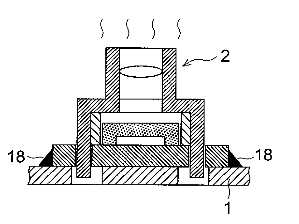
[0028]As a result, when an optical element is mounted on a substrate by a reflow treatment, a surface functional layer is not deteriorated, and it is possible to provide an optical element exhibiting a suitable refractive index and transparency.

Problems solved by technology

However, with the advancement of miniaturization of devices employing optical elements, such optical elements are required to be miniaturized.
Therefore, in view of processability, when inorganic glass materials are used, it has become difficult to produce those having large curvature (R) or a complex shape.
Since an inorganic glass material has a larger specific gravity than a plastic material, when the inorganic glass material is used as an optical element, the weight of an optical element becomes heavy.
Furthermore, when the optical element is require to be driven, a high driving voltage is needed to be set up, as a result, there is a problem that the apparatus size and power consumption become large.
On the other hand, although the thermoplastic resin which has been conventionally used as a resin material for an optical element becomes soft or melts at comparatively low temperature, it has a defect that the molded optical element will be easily deformed by the effect of heat.
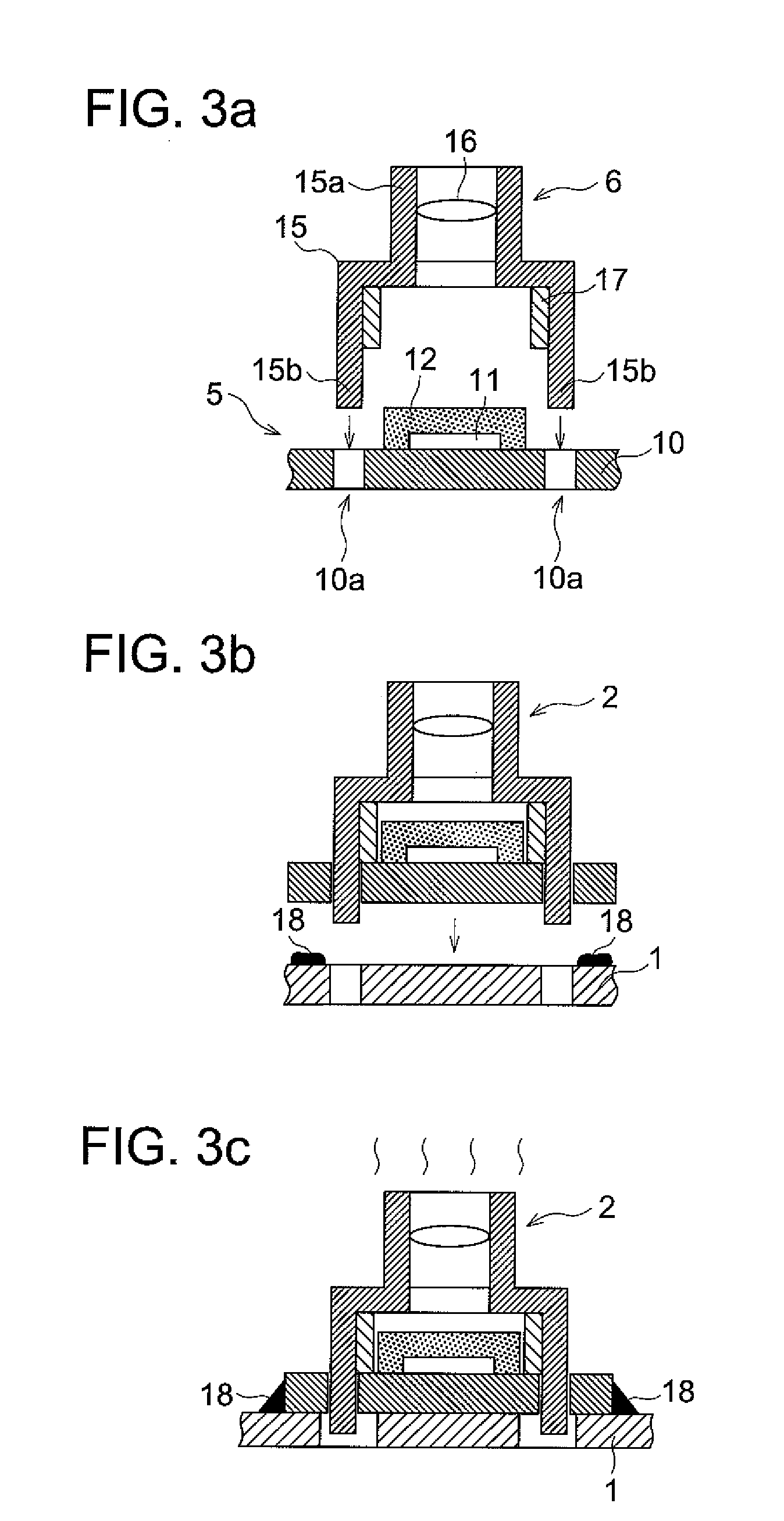
When an electronic component incorporating an optical element is mounted on a substrate by a solder reflow process, the optical element itself will be exposed to a heating condition of about 260° C., consequently, the optical element which is composed of a thermoplastic resin having a low heat resistivity will cause deterioration in shape, and it becomes a problem.
And since it is hard to melt after hardening by overheat like a thermoplastic resin, its deformation by heat is also small.
However, on the occasion of application to the reflow treatment process, there are problems of breakage or deformation of the functional layer formed on the surface of the resin base material, or coloration of the resin base material.
This technology aims at controlling the generation of crack caused by repetition of the temperature change at the time of use, and it does not aim at improvement of breakage of the functional layer at high temperature condition such as a reflow treatment process.
An object of this technology is to make a surface of an optical element smooth with a thin film containing an organic material, and this technique does not aim at the functional layer containing an inorganic compound as a main ingredient and applicable to a reflow treatment process as a main ingredient.

Method used


Image

  • Optical Element, and Process for Producing Electronic Equipment using the Optical Element
  • Optical Element, and Process for Producing Electronic Equipment using the Optical Element
  • Optical Element, and Process for Producing Electronic Equipment using the Optical Element

Examples


example 1

Preparation of Inorganic Particles 1

[0138]At first, to 23 g of TM-300 (γ alumina made by Taimei Chemicals Co., Ltd., primary particle diameter of 7 nm) were added 500 g of pure water and 4.8 g of aqueous ammonia solution (28%, made by Kanto Chemical Co., Inc.), and the mixture was stirred. This solution was dispersed with Ultra Apex Mill UAM-015 (Kotobuki Industries Co., Ltd.) using glass beads of 0.05 mm at a circumferential speed of 7 msec for fours hours. During this time, 11.5 g of tetraethoxysilane (LS-2430, made by Shin-Etsu Chemical Co., Ltd.) was dropped to the aforesaid solution over 2 hours.

[0139]From the obtained particle dispersion liquid, a portion of 327 g was taken. After adding 2,280 g of ethanol, 1,050 g of pure water and 20 g of aqueous ammonia solution (28%, made by Kanto Chemical Co., Inc.) to the aforesaid portion to dilute it, 38 g of tetraethoxysilane (LS-2430, made by Shin-Etsu Chemical Co., Ltd.) was dropped over 8 hours. Then, the liquid was agitated at roo...


PUM

PropertyMeasurementUnit
Surface roughnessaaaaaaaaaa

Abstract

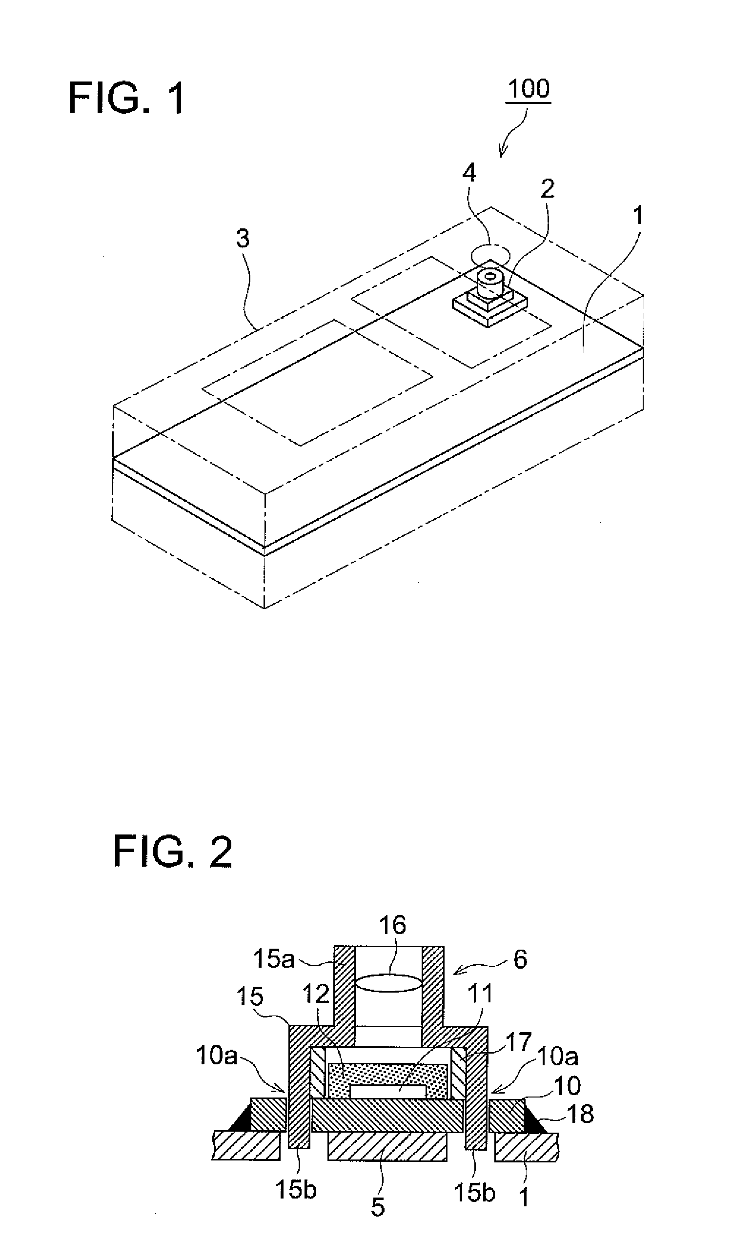
Disclosed is an optical element comprising a functional layer composed mainly of an inorganic component on a surface thereof. The functional layer provided on the surface of the optical element is not broken or deformed even through a reflow treatment process. Also disclosed is a process for producing an electronic equipment, comprising placing an image pick-up device comprising the optical element together with an electronic component on a substrate and mounting the image pick-up device and the electronic component on the substrate by a reflow treatment process. The optical element comprises a base material containing a curing resin and inorganic fine particles and a functional layer composed mainly of an inorganic component provided on the surface of the base material. The optical element is characterized in that at least one type of inorganic fine particles is present on the surface of the base material, and the surface roughness is not less than 3 nm and not more than 100 nm.

Description

TECHNICAL FIELD[0001]The present invention related to an optical element and a process for producing an electronic apparatus using the same.BACKGROUND[0002]In the past, from the viewpoint of excellent optical characteristics and mechanical strength, inorganic glass materials have been commonly used as constituent materials of optical elements (mainly lenses). However, with the advancement of miniaturization of devices employing optical elements, such optical elements are required to be miniaturized. Therefore, in view of processability, when inorganic glass materials are used, it has become difficult to produce those having large curvature (R) or a complex shape.[0003]Since an inorganic glass material has a larger specific gravity than a plastic material, when the inorganic glass material is used as an optical element, the weight of an optical element becomes heavy. Furthermore, when the optical element is require to be driven, a high driving voltage is needed to be set up, as a res...

Claims


Application Information

Patent Timeline
IPC IPC(8): B32B3/00H05K13/00
CPCG02B13/0085H01L27/14618Y10T29/49002Y10T428/24372H04N5/2251H01L2924/0002H01L2924/00
Inventor TAIMA, YASUO
Owner KONICA MINOLTA OPTO
Learn More