
Process for producing an optical waveguide and stamp for use in the production process

a technology of optical waveguides and stamps, which is applied in the direction of dough shaping, manufacturing tools, instruments, etc., can solve the problems of insufficient efficiency of manufacturing optical waveguides, and achieve the effect of simple and easy manner

Inactive Publication Date: 2011-03-31
NIPPON SHOKUBAI CO LTD
View PDF13 Cites 2 Cited by
  • Summary
  • Abstract
  • Description
  • Claims
  • Application Information

AI Technical Summary

Benefits of technology

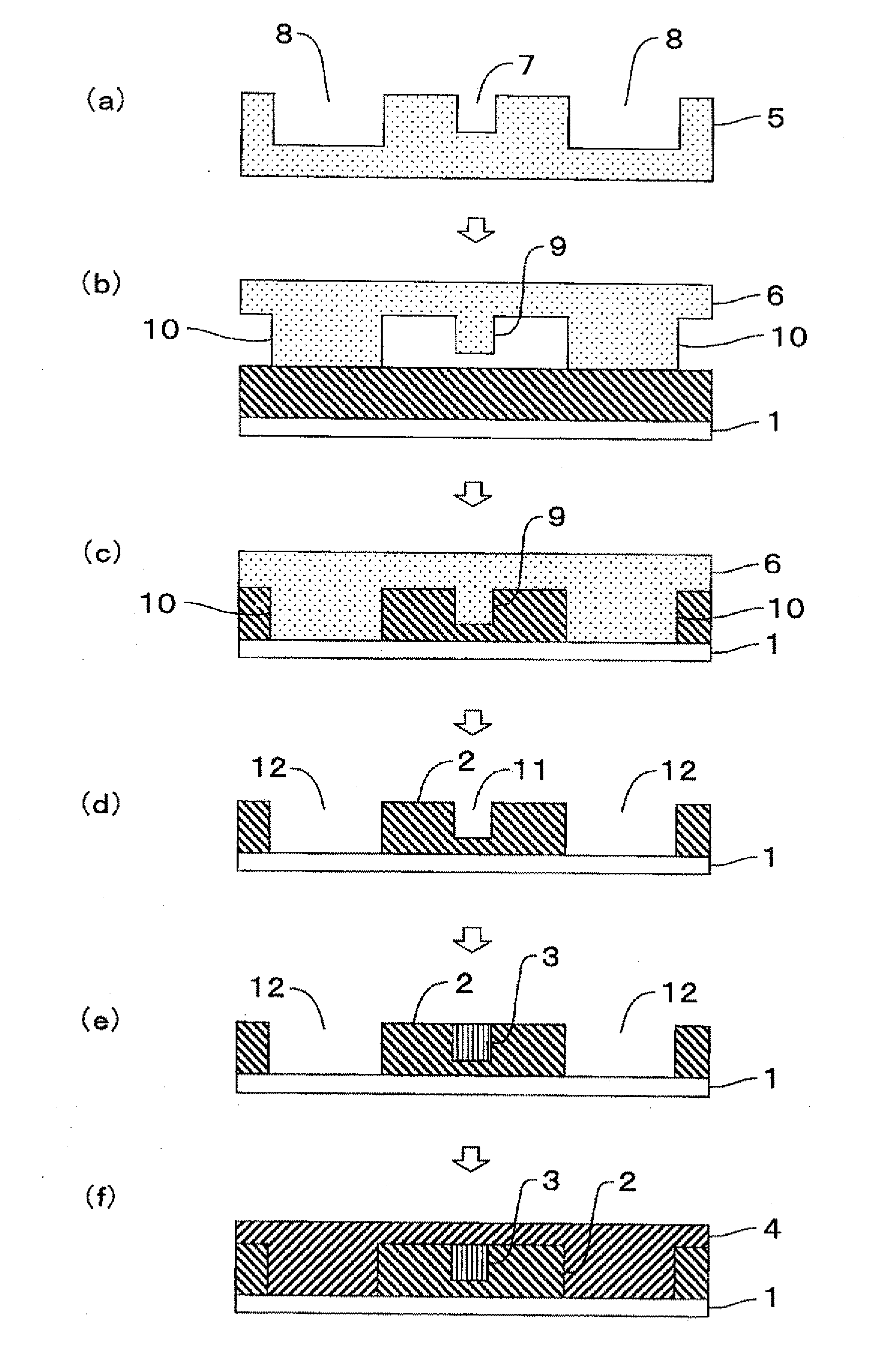
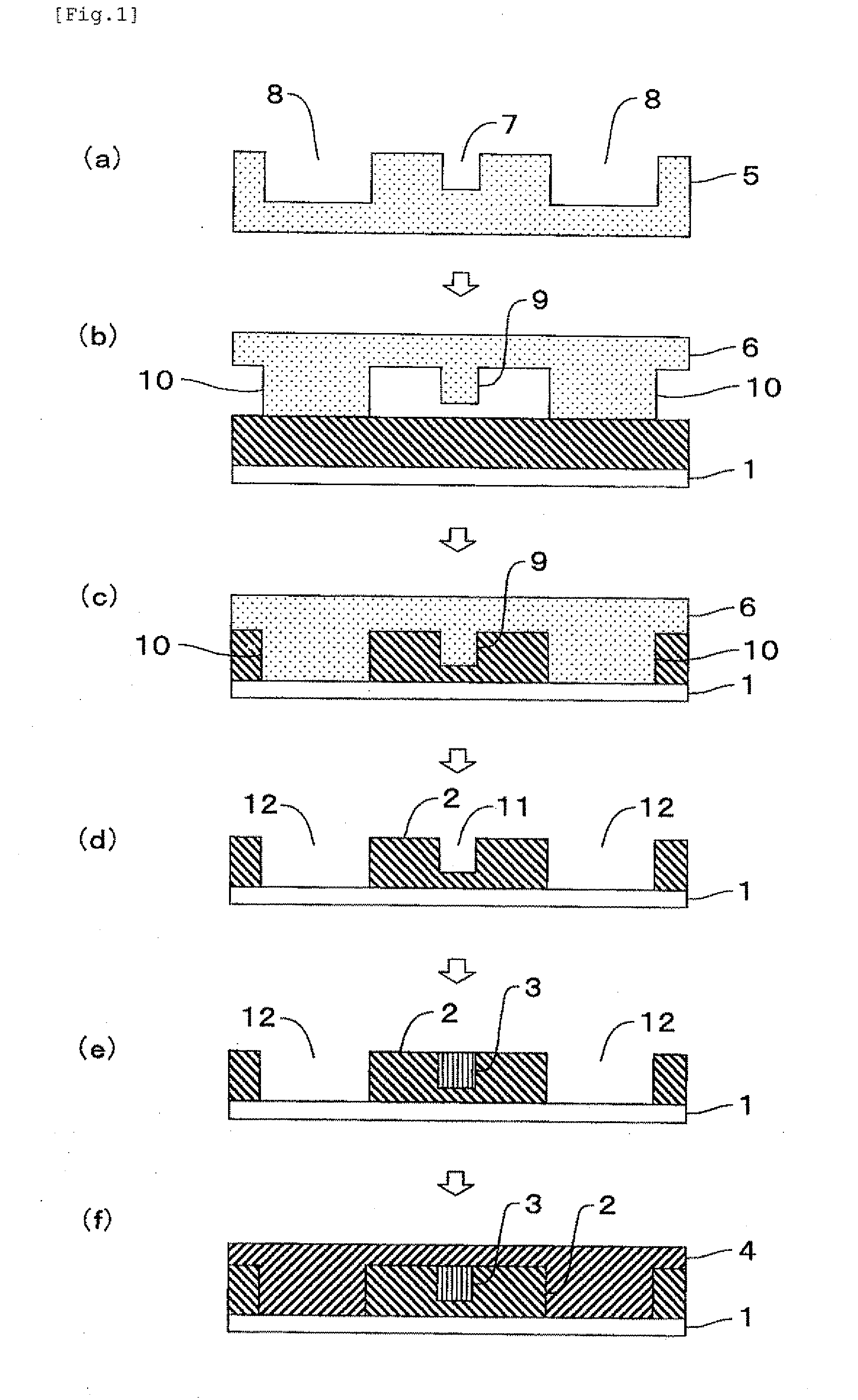
[0013]The present inventors have made various investigations and as a result, they have found that if not a male stamp having only a convex portion corresponding to a core groove, but a male stamp having a convex portion corresponding to a core groove and convex portions corresponding to spacer grooves formed substantially in parallel with intervals in both sides of the convex portion corresponding to the core groove is employed to form a lower cladding layer having a core groove and spacer grooves formed substantially in parallel with intervals in both sides of the core groove on a substrate, due to the existence of the convex portions (spacers) corresponding to the spacer grooves, the substrate or the male stamp is supported and held substantially in parallel without slacking and thus the thickness of the lower cladding layer can be easily controlled in the portion positioned in the lower side of the core layer, thereby completing the present invention.
[0019]In the process for producing the optical waveguide of the present invention, since a second stamp (a male stamp) having a convex portion corresponding to a core groove and convex portions corresponding to spacer grooves formed substantially in parallel with intervals in both sides of the convex portion corresponding to the core groove is employed to form a lower cladding layer having a core groove and spacer grooves formed substantially in parallel with intervals in both sides of the core groove on a substrate, even if a substrate with low rigidity such as a film substrate is used, or a cladding material or a stamp having a convex portion corresponding to a core groove, which are both made of a material with low rigidity, is used, an optical waveguide having a substantially uniform thickness of a lower cladding layer in the portion positioned in the lower side of a core layer and having extremely low waveguide loss can be manufactured easily.

Problems solved by technology

However, since employing a glass substrate, the above-mentioned conventional stamper methods are limited to a batch type process of manufacturing optical waveguides one by one and are inferior in the efficiency of manufacturing optical waveguides.

Method used


Image

  • Process for producing an optical waveguide and stamp for use in the production process
  • Process for producing an optical waveguide and stamp for use in the production process
  • Process for producing an optical waveguide and stamp for use in the production process

Examples


example 1

[0098]A flexible optical waveguide was produced in this Example.

[0099]1) A first stamp (a female stamp) as shown in FIG. 1(a) was produced by cutting the surface of a phosphor bronze plate (thickness of 10 mm) to form a concave portion having a width of 50 μm and a depth of 50 μm corresponding to a core groove and concave portions having a width of 1.5 mm and a depth of 75 μm corresponding to spacer grooves to be formed substantially in parallel with intervals of 100 μm in both sides of the concave portion corresponding to the core groove. In FIG. 1(a), the concave portions 8 corresponding to the spacer grooves are illustrated with their widths narrow as compared with their depths because of the drawing space.

[0100]2) A second stamp (a male stamp) made of silicone type rubber was produced by placing the first stamp on a glass substrate (thickness of 2 mm) with a space, and without introducing air bubbles, injecting and filling two-component curable silicone type rubber (trade mane, ...

example 2

[0112]A flexible optical waveguide substrate having an optical fiber fixation groove was produced in this Example.

[0113]1) A first stamp (a female stamp) was produced by cutting the surface of a phosphor bronze plate (thickness of 10 mm) to form a concave portion having a width of 50 μm and a depth of 50 μm corresponding to a core groove, concave portions having a width of 1.5 mm and a depth of 87.5 μm corresponding to spacer grooves to be formed substantially in parallel with intervals of 0.55 μm in both sides of the concave portion corresponding to the core groove, a concave portion having a width of 130 μm and a depth of 112.5 μm corresponding to an optical fiber fixation groove, and a convex portions having a thickness of 50 μm and a height of 112.5 μm corresponding to the weir between the concave portion corresponding to the core groove and the concave portion corresponding to the optical fiber fixation groove.

[0114]2) A second stamp (a male stamp) made of silicone type rubber ...


PUM

PropertyMeasurementUnit
Thicknessaaaaaaaaaa
Depthaaaaaaaaaa
Stiffnessaaaaaaaaaa

Abstract

In an optical waveguide, the present invention provides a process for producing an optical waveguide, and a stamp for use in the production process, in which the thickness of a lower cladding layer in the portion positioned in the lower side of a core layer is easily controlled even if any one or more materials of a substrate, a cladding material, and a stamp are material with low rigidity. The production process of the present invention comprises steps of forming a lower cladding layer which has a core groove and spacer grooves formed substantially in parallel with intervals in both sides of the core groove on a substrate by making use of soft lithography with a second stamp (i.e., a male stamp); then forming a core layer by injecting and filling a core material into the core groove, followed by curing the core material; further forming a upper cladding layer by injecting and filling a cladding material into the spacer grooves and applying the cladding material to the lower cladding layer so as to be embedded the core layer and followed by curing. A stamp used in the production process of the present invention comprises a convex portion or a concave portion corresponding to a core groove and convex portions or concave portions corresponding to spacer grooves formed substantially in parallel with intervals in both sides of the convex portion or the concave portion corresponding to the core groove.

Description

TECHNICAL FIELD[0001]The present invention relates to a process for producing an optical waveguide and a stamp for use in the production process.BACKGROUND ART[0002]Along with the practical applications of optical transmission systems, techniques relevant to optical waveguides as their basic components have drawn much attention. An optical waveguide has, typically, an embedded type structure in which a core layer having a high refractive index is surrounded with a cladding layer having a low refractive index, or a ridge type structure in which a core layer having a high refractive index is formed on a lower cladding layer having a low refractive index and an upper cladding layer is an air layer. Thus, light incoming to the optical waveguide is transmitted in the core layer while being reflected at the interface between the core layer and the cladding layers or at the interface between the core layer and the air layer.[0003]As an optical waveguide production process, for example, a m...

Claims


Application Information

Patent Timeline
IPC IPC(8): G02B6/13B28B11/10
CPCG02B6/138G02B1/045
Inventor TAJIRI, KOZOMAKINO, TOMOMI
Owner NIPPON SHOKUBAI CO LTD
Learn More