Semiconductor device
a technology of semiconductor devices and semiconductors, applied in semiconductor devices, semiconductor/solid-state device details, electrical apparatus, etc., can solve the problems of increasing deteriorating characteristics, and achieve the effect of reducing the loss in the transmission line, improving the signal transmission efficiency of the transmission line, and shortening the distance between an element such as a transistor and the signal lin
- Summary
- Abstract
- Description
- Claims
- Application Information
AI Technical Summary
Benefits of technology
Problems solved by technology
Method used
Image

Examples
first embodiment
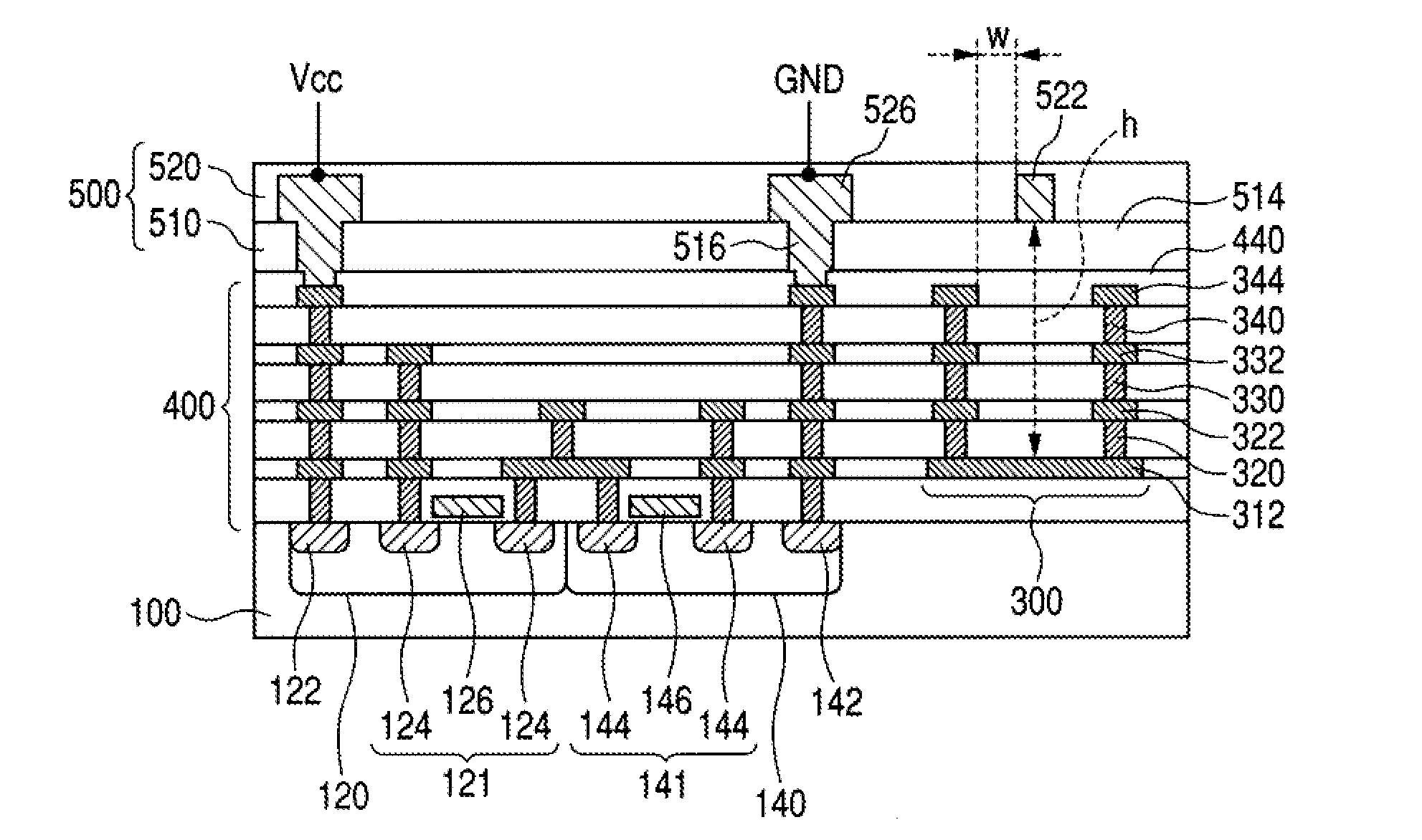
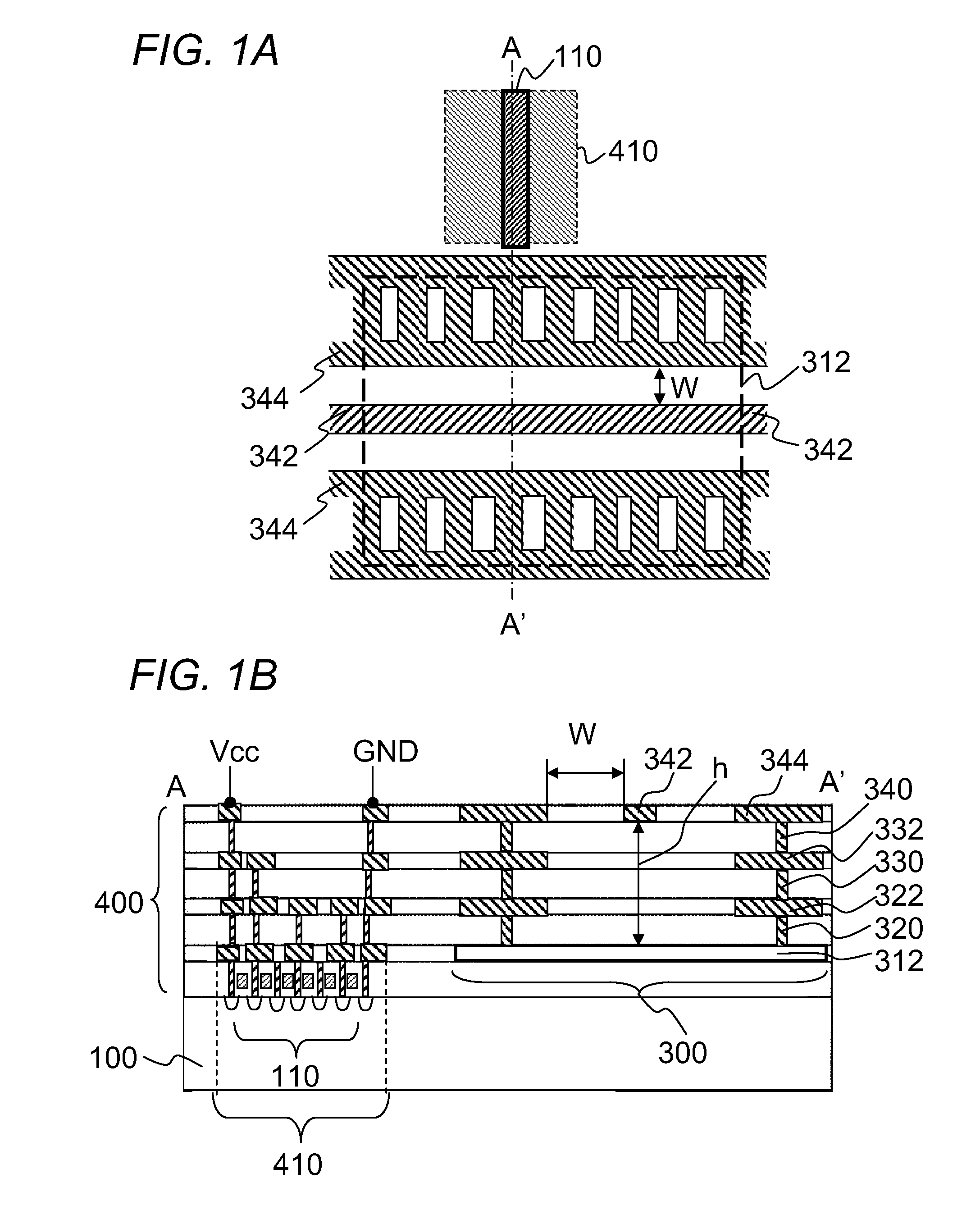
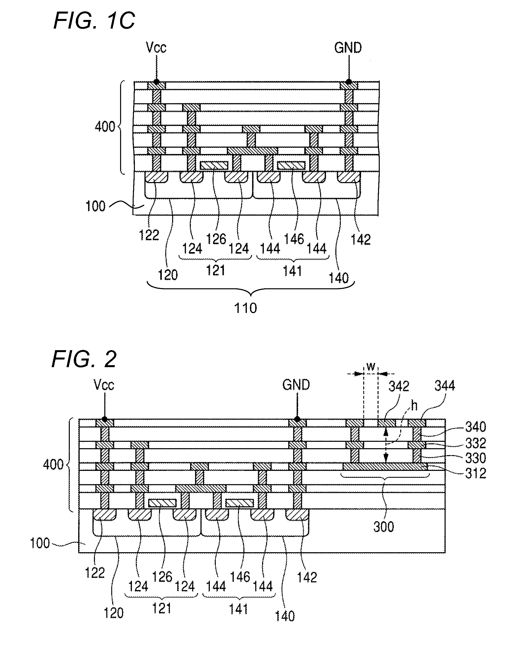
[0053]This embodiment brings about the same effects as the Also, since the width of the second conductor patterns 344, 332, and 322 is larger than that of the signal line 342, the shield effect of the second conductor patterns 344, 332, and 322 is higher. Also, the first vias 340, 330, and 320 are each provided in a plurality when viewed in the width direction of the second conductor patterns 344, 332, and 322, so the resistance between the first conductor pattern 312 and the second conductor patterns 344, 332, and 322 is lower. Therefore, the signal transmission efficiency of the transmission line 300 is further increased.
[0054]In the first embodiment, the width of the second conductor patterns 344, 332, and 322 may be larger than the width of the signal line 342, as in the second embodiment.
third embodiment
[0055]FIG. 4 is a sectional view of a semiconductor device according to the invention. The transistor region 110 as illustrated in FIG. 4 omits some of the actual number of transistors for clarity. This semiconductor device is structurally the same as the semiconductor device shown in FIG. 2 except that the transistor region 110 overlaps the first conductor pattern 312 of the transmission line 300 in a plan view. The top view of the semiconductor device of this embodiment is same as that of FIG. 12B.
[0056]More specifically, in this embodiment, the transistor region 110 lies under the transmission line 300. Therefore, the interconnect wiring used to couple the transistors to the transmission line can be shorter than when the transistor region 110 is formed in a different region from the transmission line 300. Therefore, loss in the transmission line can be decreased and the signal transmission efficiency of the transmission line of the semiconductor device can be improved. In additio...
fifth embodiment
[0073]This embodiment also brings about the same effects as the The absence of the second conductor patterns 524 in the same layer as the signal line 522 allows more freedom in the arrangement of interconnects in the same layer as the signal line 522.
[0074]FIG. 10 is a sectional view of a semiconductor device according to an eighth embodiment of the invention. Nevertheless, FIG. 10 depicts the semiconductor region on a substantially larger horizontal scale than the transmission line 300, for ease of understanding. This semiconductor device is structurally the same as the semiconductor device according to the first embodiment except that it has no second conductor patterns 342, 332, and 322 and first vias 340, 330, and 320. In other words, the transmission line 300 in this embodiment is a microstrip line.
[0075]In this embodiment as well, the height from the first conductor pattern 312 to the signal line 342 is sufficient so that the impedance of the transmission line 300 can be high...
PUM
 Abstract
Description
Claims
Application Information
 - R&D
- Intellectual Property
- Life Sciences
- Materials
- Tech Scout
- Unparalleled Data Quality
- Higher Quality Content
- 60% Fewer Hallucinations
Browse by: Latest US Patents, China's latest patents, Technical Efficacy Thesaurus, Application Domain, Technology Topic, Popular Technical Reports.
© 2025 PatSnap. All rights reserved.Legal|Privacy policy|Modern Slavery Act Transparency Statement|Sitemap|About US| Contact US: help@patsnap.com