Optical transmission module

a transmission module and optical transmission technology, applied in the direction of optics, optical waveguide light guide, instruments, etc., can solve the problems of inconvenient use of specific materials, inability to meet the requirements of conventional metallic transmission lines, and complicated arrangement of electronic component layers and photonic layers at the same side, so as to improve the signal transmission efficiency of optical transmission modules and simplify the manufacturing process

Active Publication Date: 2014-03-04
NAT CENT UNIV
View PDF22 Cites 10 Cited by
  • Summary
  • Abstract
  • Description
  • Claims
  • Application Information

AI Technical Summary

Benefits of technology

[0010]Therefore, the object of the present invention is to provide an optical transmission module for converting and transmitting electrical signals or optical signals by using a waveguide structure to allow the optical signals to undergo total internal reflection. Consequently, the electronic component layer and the photonic layer arranged at different sides of the optical transmission module can be connected with each other in a simplified fabricating process. Since the optical transmission module is mainly used to emit, convert and receive optical signals, the problems of installing the vertical channel and the metallic lines will be overcome. In addition, the signal transmission efficiency of the optical transmission module is enhanced.

Problems solved by technology

However, the conventional metallic transmission lines fail to meet these requirements.
In addition, since the fabricating processes of the electronic component layer and the photonic layer are usually different or incompatible, it is complicated to arrange the electronic component layer and the photonic layer at the same side.
However, the use of the specific material is not cost-effective and the fabricating process needs to be elaborately adjusted.
However, it is difficult to install the metallic lines 121 and 122 in the metallic interconnection structure 12.
However, it is difficult to install the metallic lines 221 and 222 in the silicon substrate.
In other words, the volume of the optical transmission module 20 is bulky.

Method used


Image

  • Optical transmission module
  • Optical transmission module
  • Optical transmission module

Examples


Embodiment Construction

[0021]The present invention will now be described more specifically with reference to the following embodiments. It is to be noted that the following descriptions of preferred embodiments of this invention are presented herein for purpose of illustration and description only. It is not intended to be exhaustive or to be limited to the precise form disclosed.

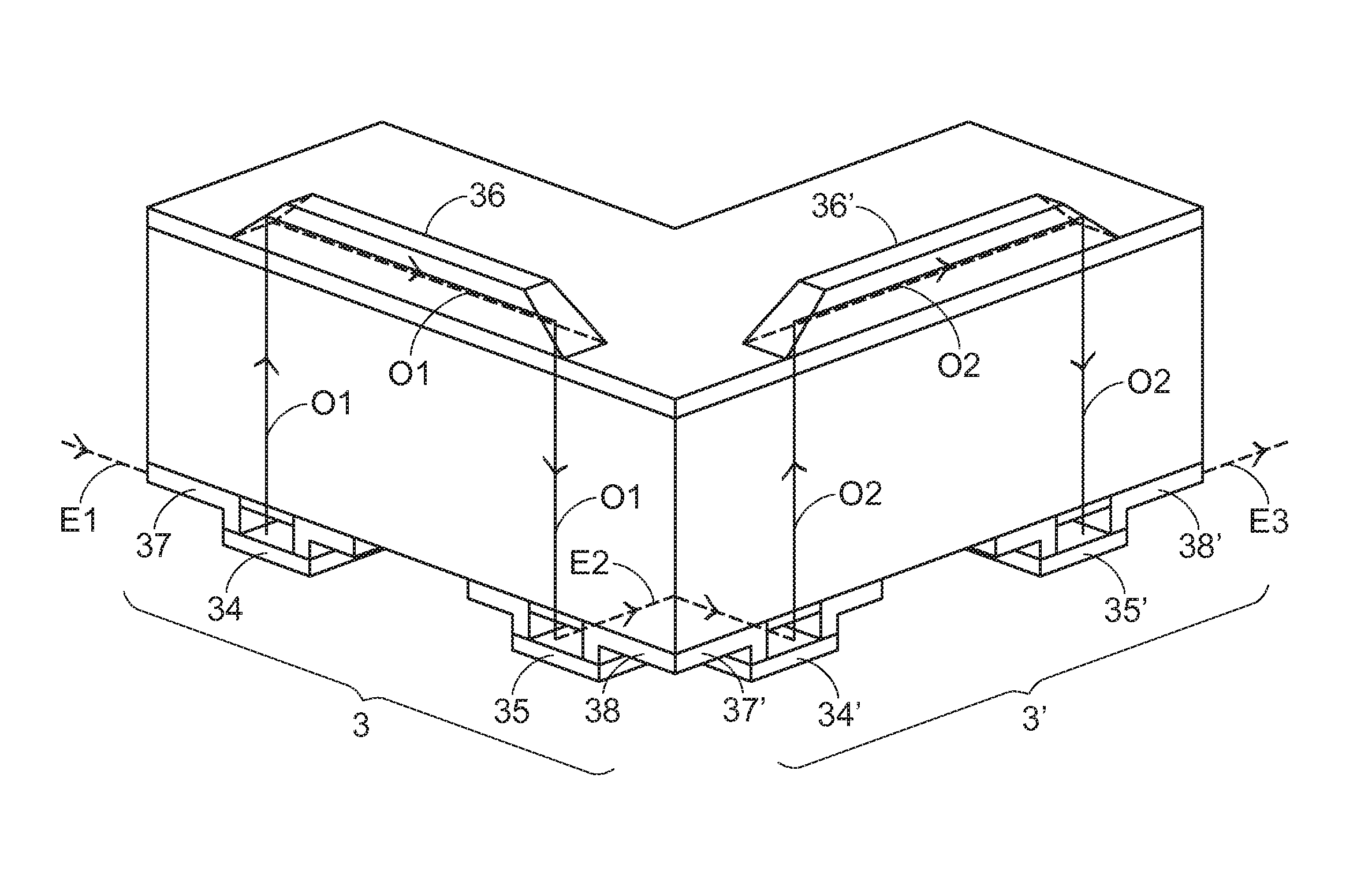
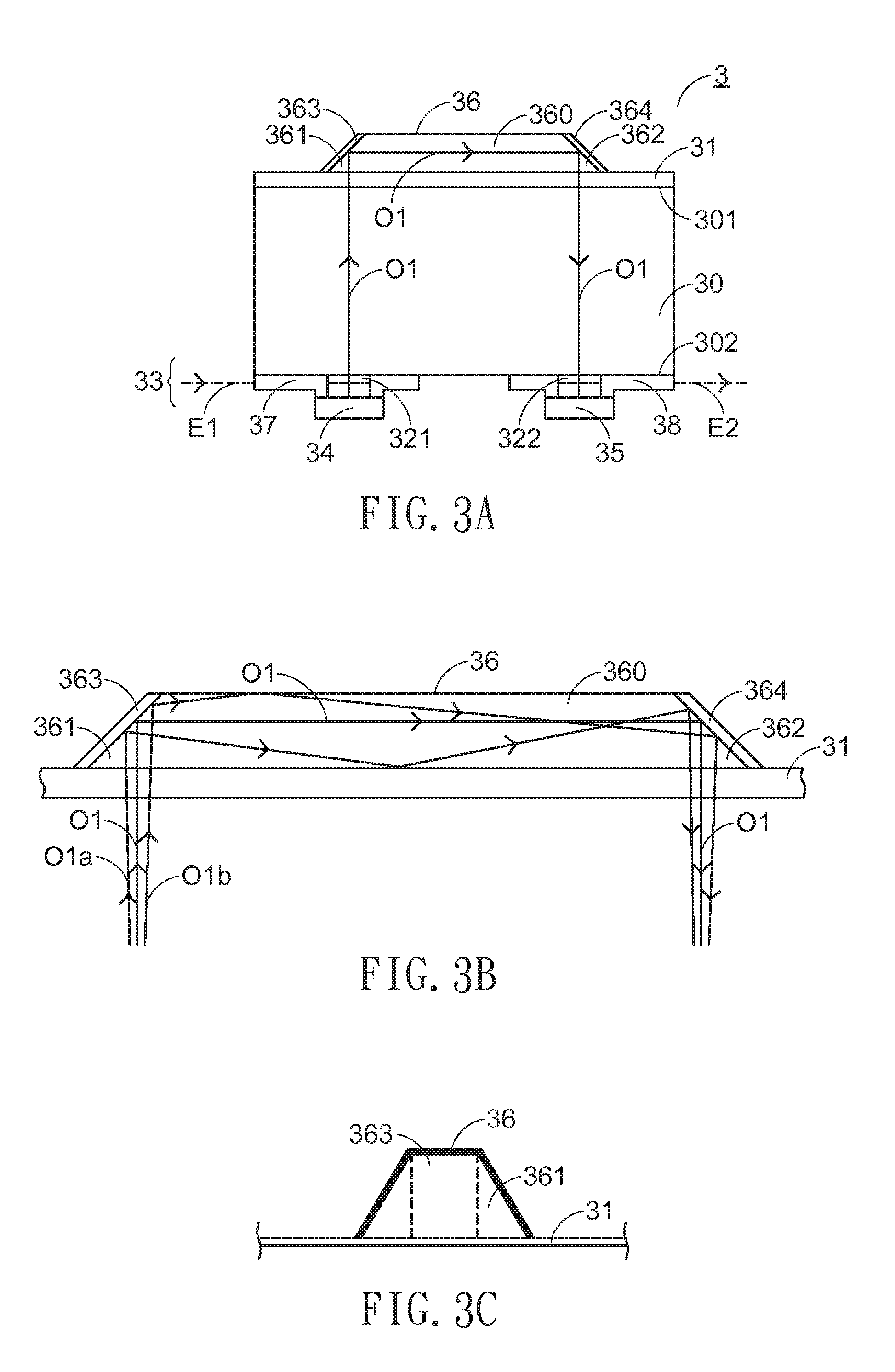
[0022]FIG. 3A is a schematic cross-sectional view illustrating an optical transmission module according to a first embodiment of the present invention. As shown in FIG. 3A, the optical transmission module 3 includes a semiconductor substrate 30, a first film layer 31, an electronic component layer 33 and a waveguide structure 36. The semiconductor substrate 30 has two opposite surfaces: a first surface 301 (i.e. a top surface) and a second surface 302 (e.g. a bottom surface). The first film layer 31 and the electronic component layer 33 are formed on the first surface 301 and the second surface 302 of the semiconductor substrate ...


PUM


Abstract

An optical transmission module includes a semiconductor substrate, a first film layer, an electronic component layer and a waveguide structure. The electronic component layer is used for converting a first electrical signal into an optical signal. The waveguide structure is formed on the first film layer, and includes a first reflective surface, a waveguide body and a second reflective surface. After the optical signal is transmitted through the semiconductor substrate and the first film layer and enters the waveguide structure, the optical signal is reflected by the first reflective surface, transmitted within the waveguide body and reflected by the second reflective surface. After the optical signal reflected by the second reflective surface is transmitted through the first film layer and the semiconductor substrate and received by the electronic component layer, the optical signal is converted into a second electrical signal by the electronic component layer.

Description

FIELD OF THE INVENTION[0001]The present invention relates to an optical transmission module, and more particularly to an optical transmission module for converting and transmitting electrical signals or optical signals by using a waveguide structure to allow the optical signals to undergo total internal reflection.BACKGROUND OF THE INVENTION[0002]Conventionally, metallic transmission lines are widely used to transmit electrical signals or data between different components. In a high performance electronic system, since more and more processors are utilized and the signal processing speed is enhanced, it is important to enhance the quality and speed of transmitting the signals and data. However, the conventional metallic transmission lines fail to meet these requirements.[0003]As known, there is almost no adverse influence of the material of the transmission line on the optical connection. Consequently, the optical signals may be transmitted at a high bandwidth and a high speed. Rece...

Claims


Application Information

Patent Timeline
Patent Type & Authority Patents(United States)
IPC IPC(8): G02B6/12
CPCG02B6/4214G02B6/43
Inventor WU, MAO-JENLAN, HSIAO-CHINLEE, YUN-CHIHCHANG, CHIA-CHIHSIAO, HSU-LIANGCHEN, CHIN-TASHEN, BO-KUANLU, GUAN-FUCHANG, YAN-CHONGCHANG, JEN-YU
Owner NAT CENT UNIV
Why Eureka
Try Eureka