OLED display panel with pwm control

a display panel and control technology, applied in the field of display panels, can solve the problems of difficult cost reduction, complex manufacturing process of transistors, non-uniform display, etc., and achieve the effect of effective control of curren

Inactive Publication Date: 2011-04-14
GLOBAL OLED TECH
View PDF3 Cites 53 Cited by
  • Summary
  • Abstract
  • Description
  • Claims
  • Application Information

AI Technical Summary

Benefits of technology

[0008]According to the present invention, an emission period can be controlled, and also current can be controlled effectively according to image data. Further, as the drain of the reset transisto

Problems solved by technology

In the case of driving transistors with a constant current, as they are used in a saturated region, variation in the characteristics of the transistors such as thresholds and mobility causes variation in the c

Method used


Image

  • OLED display panel with pwm control
  • OLED display panel with pwm control
  • OLED display panel with pwm control

Examples


Embodiment Construction

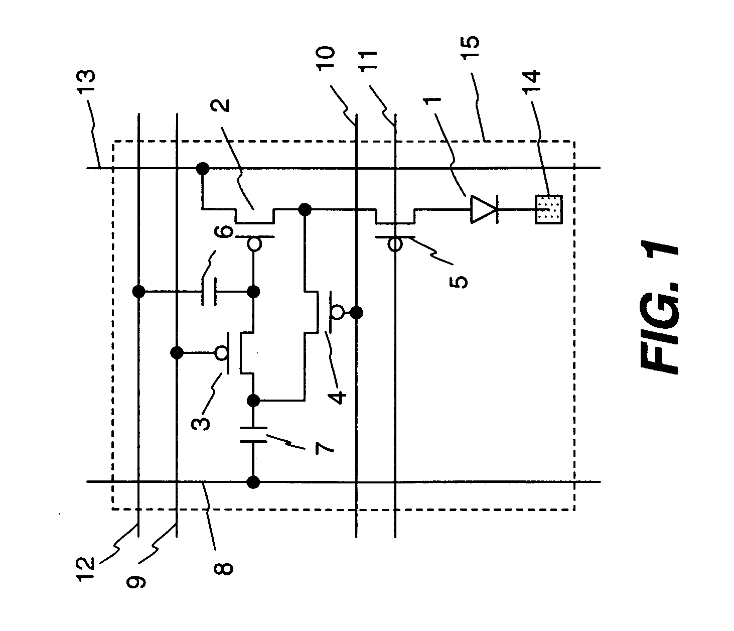
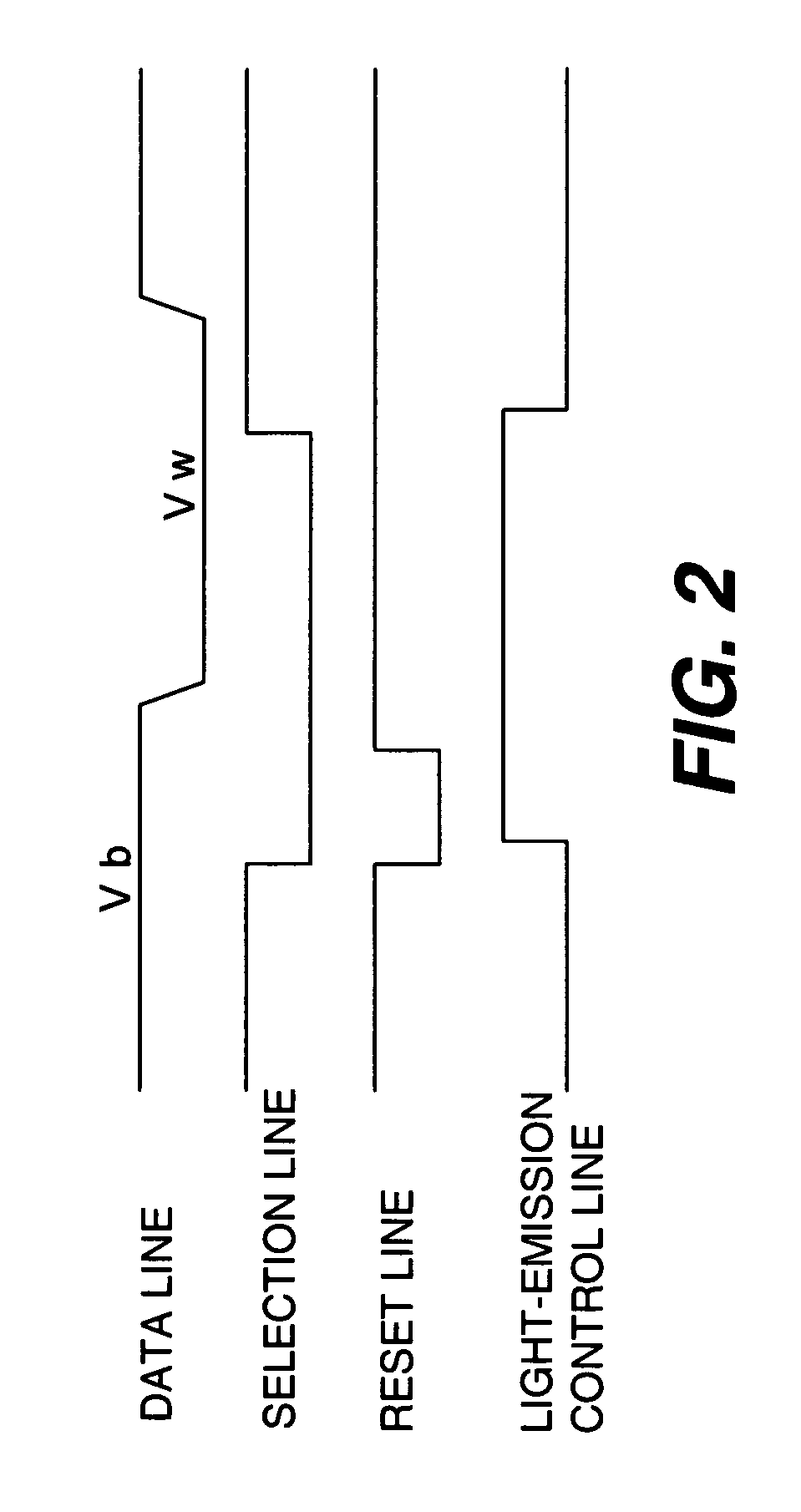
[0017]Hereinafter, an embodiment of the present invention will be described with reference to the drawings.

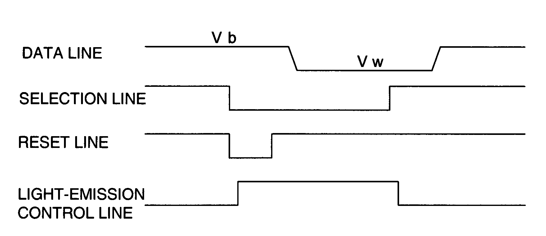
[0018]FIG. 1 shows an exemplary configuration of a pixel 15 in a display according to an embodiment. The pixel 15 includes an organic EL element 1, a drive transistor 2, a selection transistor 3, a reset transistor 4, a light-emission control transistor 5, a storage capacitor 6, and a coupling capacitor 7. It should be noted that a P-type thin film transistor is adopted for every transistor.

[0019]The drive transistor 2 is configured such that its source terminal is connected to a power source line 13 shared by all pixels, its drain terminal is connected to the source terminal of the light-emission control transistor 5 and to the source terminal of the reset transistor 4, and its gate terminal is connected to one end of the storage capacitor 6 and the source terminal of the selection transistor 3, the other end of the storage capacitor 6 being connected to a sweep line 12. The g...


PUM


Abstract

A display panel which applies a PWM drive to a drive transistor (2) is provided. A drive transistor supplies current in accordance with its gate voltage, and the current is supplied to a light-emitting element (1) to illuminate the light emitting element. One end of a storage capacitor (6) is connected to the gate of the drive transistor, while the other end thereof is connected to a sweep line (12). A triangular wave which alternately repeats an up phase and a down phase is supplied to the sweep line in order to control an on period of the drive transistor in accordance with the gate voltage, to thereby control light emission of the light-emitting element.

Description

FIELD OF THE INVENTION[0001]The present invention relates to a display panel having pixels arranged in a matrix.BACKGROUND OF THE INVENTION[0002]As organic EL displays are self-emissive, they exhibit high contrast and quick response, making them suitable for video applications such as televisions which display natural images and the like. In general, an organic EL element is driven by way of control elements such as transistors, in which multiple tones are realized by driving transistors with a constant current according to data, or by driving transistors with a constant voltage so as to change the emission period.[0003]In the case of driving transistors with a constant current, as they are used in a saturated region, variation in the characteristics of the transistors such as thresholds and mobility causes variation in the current flowing through an organic EL element, which results in non-uniformity in display. As such, JP 2007-79599A discloses a method of reducing non-uniformity ...

Claims


Application Information

Patent Timeline
IPC IPC(8): G09G3/32G09G5/10
CPCG09G3/2014G09G3/3233G09G3/3258G09G3/3266G09G2320/043G09G2300/0852G09G2300/0861G09G2300/0876G09G2310/066G09G2300/0819
Inventor KAWABE, KAZUYOSHI
Owner GLOBAL OLED TECH
Why Eureka
Try Eureka