Interposer Based Monolithic Microwave Integrate Circuit (iMMIC)

a monolithic microwave and integrated circuit technology, applied in the direction of electrical equipment, semiconductor devices, semiconductor/solid-state device details, etc., can solve the problems of large area consumed by transmission line networks, disadvantageous 1 mm line length,

Inactive Publication Date: 2011-04-21
TELEDYNE SCI & IMAGING
View PDF12 Cites 24 Cited by
  • Summary
  • Abstract
  • Description
  • Claims
  • Application Information

AI Technical Summary

Problems solved by technology

At 44 GHz, this represents a disadvantageously long 1 mm line length.
These transmission line networks consume large areas of expensive heterostructure wafer material in traditional MMICs.

Method used


Image

  • Interposer Based Monolithic Microwave Integrate Circuit (iMMIC)
  • Interposer Based Monolithic Microwave Integrate Circuit (iMMIC)
  • Interposer Based Monolithic Microwave Integrate Circuit (iMMIC)

Examples


Embodiment Construction

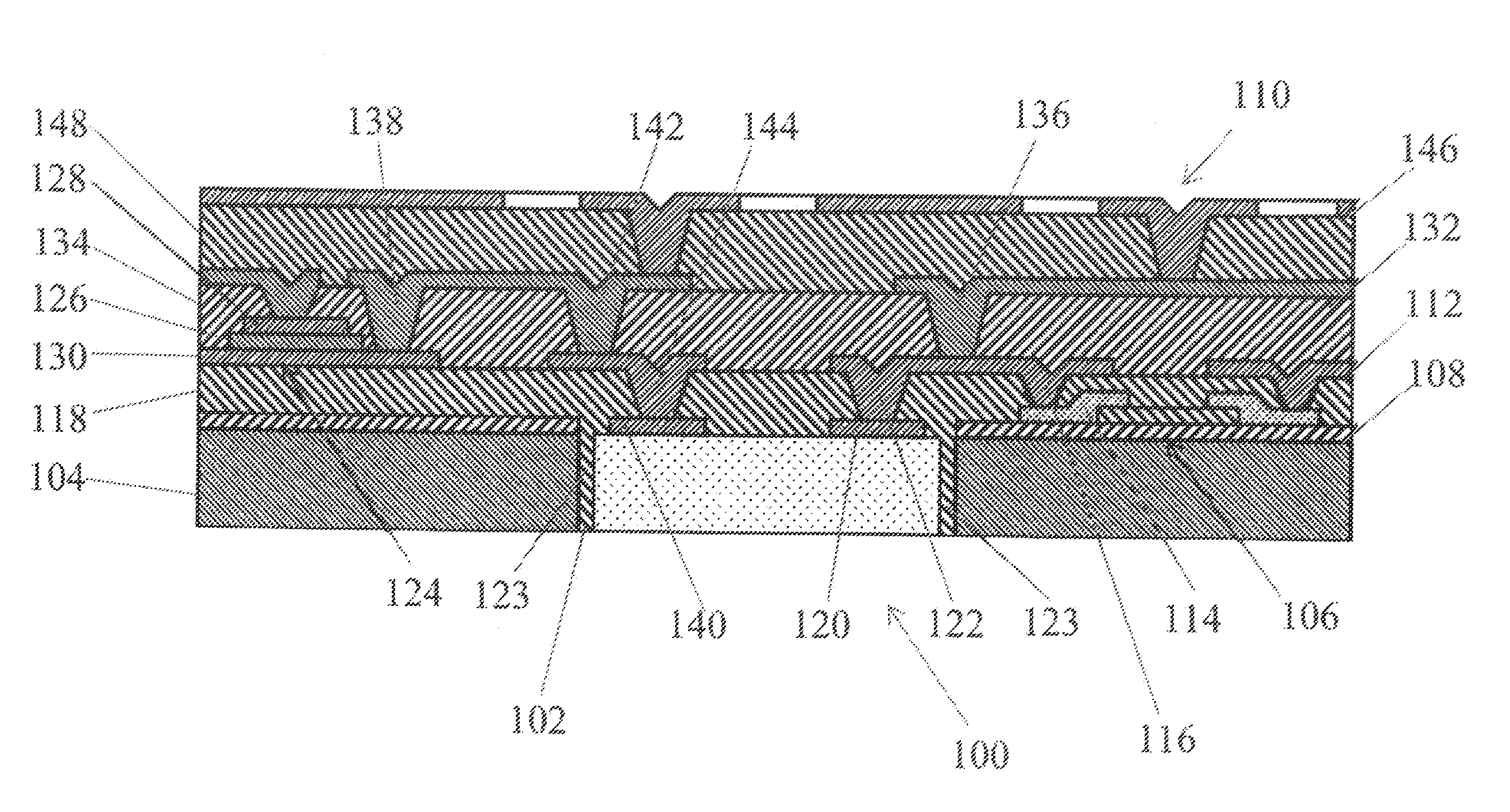
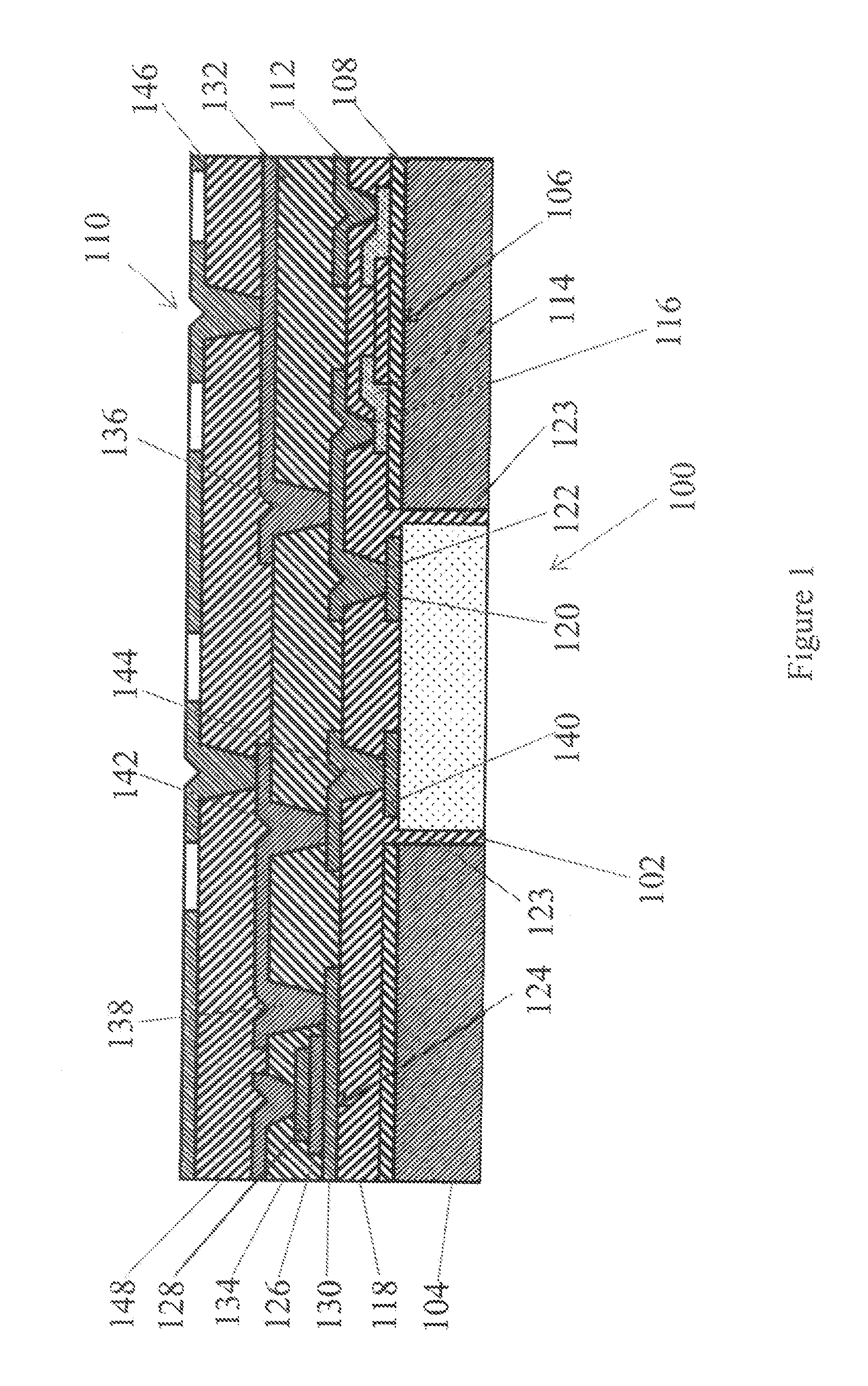
[0023]A method for fabricating an integrated circuit interposer, in accordance with one embodiment, includes seating an IC in a recess of a silicon interposer substrate and providing a low stress Benzocyclobutene (“BCB”) film in the recess and over both the seated IC and silicon interposer substrate. The novel low stress process enables thicker BCB films than previously obtained in the art in a process suitable for circuit level batch fabrication.

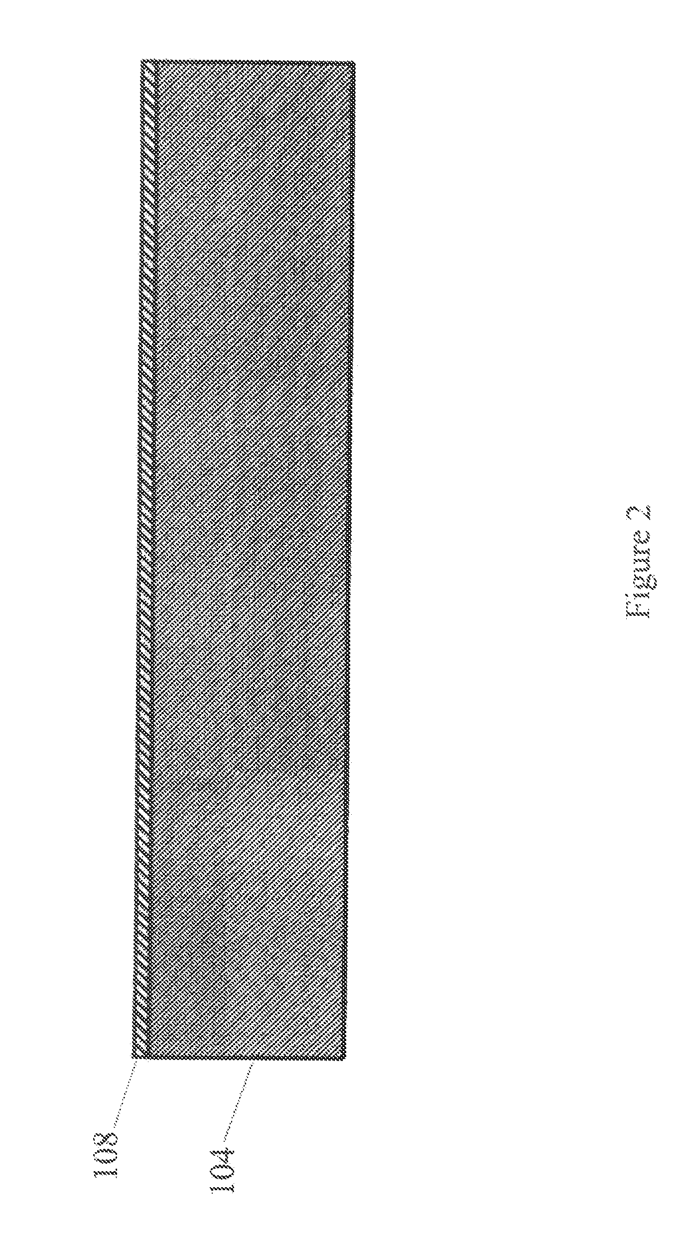
[0024]FIG. 1 illustrates one embodiment of an MMIC 100 fully seated in a recess 102 of an interposer substrate, preferably a silicon interposer substrate 104, with the recess 102 preferably extending entirely through the silicon interposer substrate. A device such as a thin film resistor (TFR) 106 preferably sits on the silicon interposer substrate 104 through a dielectric insulator layer 108 as part of a power combining and matching network (not shown). In alternative embodiments, the recess 102 may extend only partially through the silico...


PUM


Abstract

A system is disclosed for IC fabrication, including seating an integrated circuit (“IC”) having at least one contact into a recess of a silicon interposer substrate, applying an insulator in liquid form to fill portions of the recess not otherwise occupied by the IC and to cover a top surface of the IC and the silicon interposer substrate, introducing the insulator to a ramped environmental temperature, holding the environmental temperature at a reflow temperature to reflow the insulator and ramping down the environmental temperature to cure the insulator.

Description

[0001]This application claims the benefit of U.S. Provisional Application No. 61 / 252,547 filed on Oct. 16, 2009.BACKGROUND OF THE INVENTION[0002]1. Field of the Invention[0003]The present invention relates generally to integrated circuit interposers and packaging, and more particularly to Monolithic Microwave Integrated Circuits (MMIC) that utilize interposers.[0004]2. Description of the Related Art[0005]Emerging 3D System-in-Chip packaging approaches require MMIC circuits to function properly when buried deep inside dielectric packages without signal degradation, circuit detuning, or signal leakage and cross-talk.[0006]Power amplifier die area is dominated by the area used for impedance matching and power-combining networks. Matching networks require approximately 1-3 lines having a length of approximately λd / 4 on both input and output, while N:1 power combiners require roughly N transmission lines also having a length of approximately λ / 4. At 44 GHz, this represents a disadvantage...

Claims


Application Information

Patent Timeline
Patent Type & Authority Applications(United States)
IPC IPC(8): H01L29/92H01L21/56
CPCH01L23/5389H01L2924/01023H01L2224/24227H01L2224/92H01L2224/92244H01L2924/01079H01L2924/10329H01L2924/15153H01L2924/15165H01L2924/3011H01L24/82H01L2924/01019H01L2924/01006H01L2924/13064H01L24/24H01L2924/014H01L2924/01033H01L2924/01005H01L2224/83H01L2224/82H01L2924/00H01L2924/14H01L2224/04105H01L2224/73267
Inventor HILLMAN, CHRISTOPHER E.HACKER, JONATHAN B.HA, WONILLNEWELL, SCOTTTRAN, LAN
Owner TELEDYNE SCI & IMAGING
Why Eureka
Try Eureka